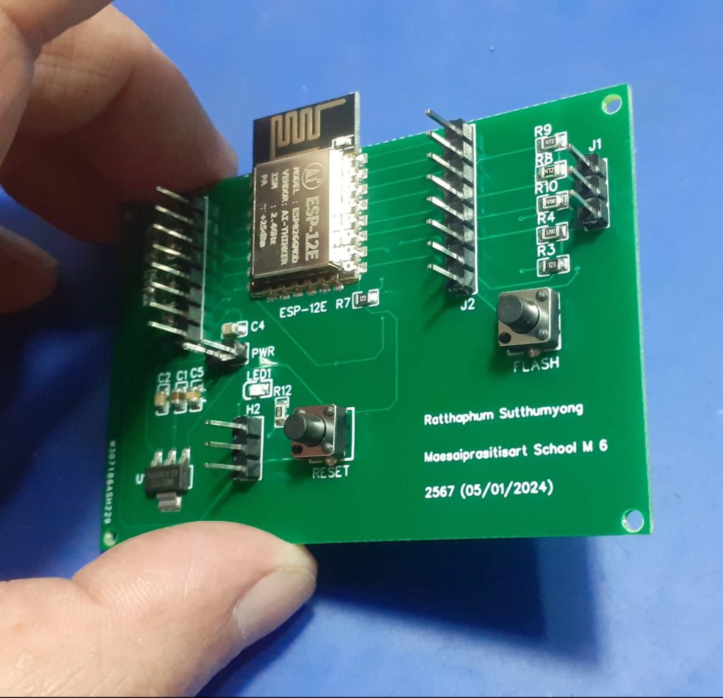
A Student designed ESP8266 Dev Board

This is a student-designed ESP8266 Dev board. This project came along after I challenged some final-year students at our local high school to try to design their own PCBs. They had recently assisted me in a collaboration with the Mushroom House Controller project, and while we were talking about electronics, the idea of a challenge came up, to stimulate some interaction.
One of them was extremely confident that he could do it, providing that I gave him a schematic. I complied, and he spent the next week hacking away on the EDA software. When i saw him again, he very proudly handed me a USB flash drive, containing the EDA design, but no schematic! Oh well, let us take a chance and see what happens… I mean, how bad could it be…
I took a good look at the design, making sure that it was at least electrically sound, with all the connections made to the right components, in the right way.
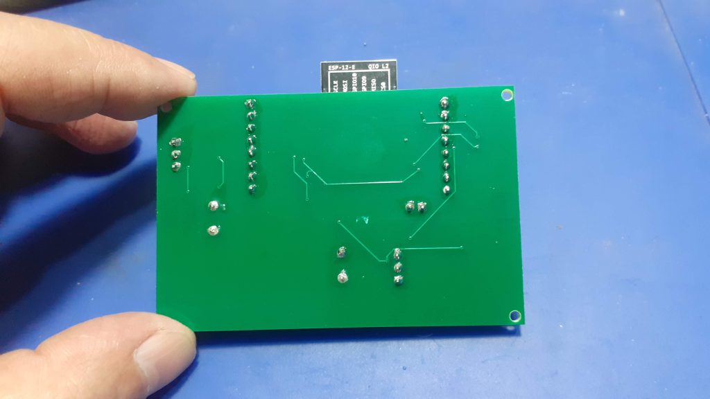
That part all passed, but, as we can clearly see, the layout could be very much improved. I decided to NOT change anything on the PCB, to keep the work original.
Manufacturing the PCB
The PCB for this project was sponsored by PCBWay .
Disclaimer:
Clicking on the PCBWay link will take you to the PCBWay website. It will enable you to get a $5.00 USD voucher towards your first PCB order. (Only if you sign up for a free account).
Assembly
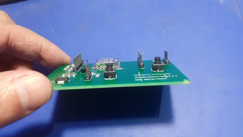
The PCB was assembled with help of a stencil.
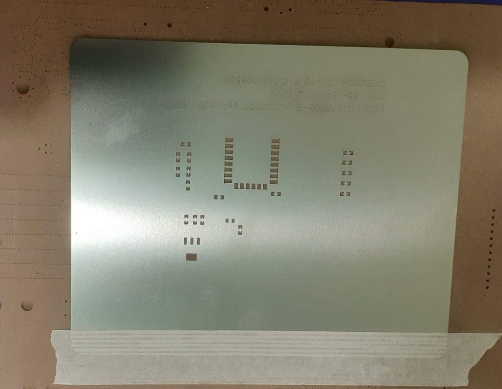
Technically, this PCB does not actually need it, as the components are large enough to manually place solder paste. This being a student project, I did however choose to get the stencil to try and assure the best possible chance of success…
Placing components only took a few minutes, after which the PCB was reflowed with hot air – no need for a hotplate here!
Through-hole components took only another few minutes to solder into place, and then testing could commence.
My thoughts – a very “gentle” critique
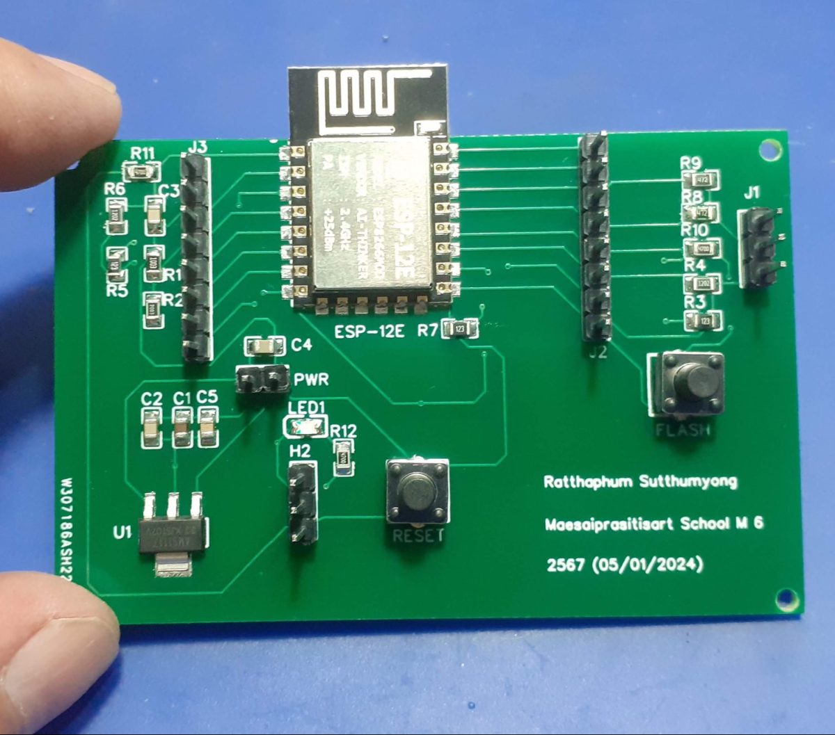
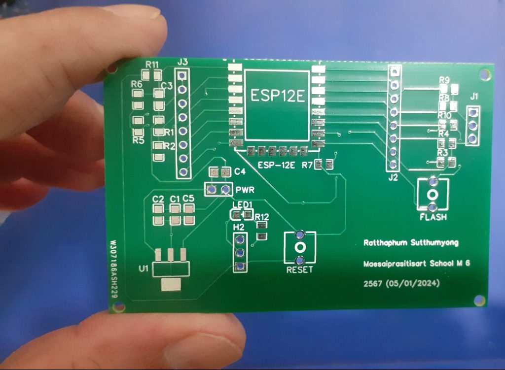
The board could be smaller, but due to the fact that this is a “very first PCB ever” and also a first SMD PCB at that, I can understand that it may still be quite difficult to understand how small the components really are, as well as lay them out properly.
Components are mostly all over the board, without a clear “group by function” kind of mindset. This once again comes back to experience.
GPIO pins are not notated. This will really make the board difficult to use.
The power supply input is in the center of the PCB. This is definitely not ideal.
In general, track sizes could have been bigger, especially on the Power and Ground lines. No ground plane was poured on either layer.
So does it work?
Yes, surprisingly it does. We shall see more of it in the near future, when I task the creator with using it to perform some task. That way, he can experience first hand the difficulties of the design, and also learn practically why certain things need to be improved.