Originally shared by John Lauer
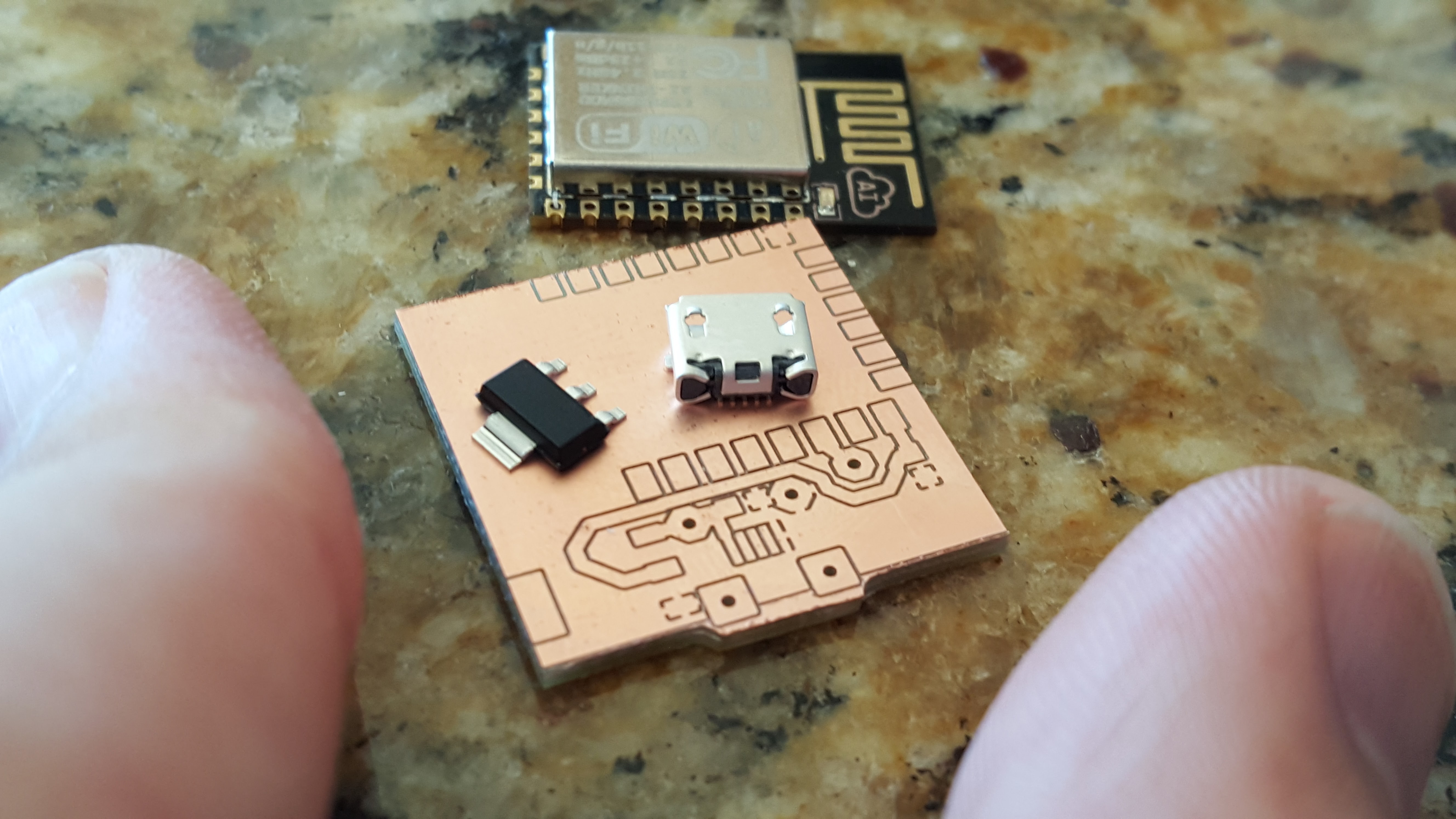
Best results in history for me milling detailed circuit boards. Combo of 3040 CNC rigidity, ChiliPeppr Eagle BRD Import and Auto-Leveller, and http://precisebits.com’s tapered stub 0.13mm dia endmill.
Originally shared by John Lauer
Best results in history for me milling detailed circuit boards. Combo of 3040 CNC rigidity, ChiliPeppr Eagle BRD Import and Auto-Leveller, and http://precisebits.com’s tapered stub 0.13mm dia endmill.
This is one of my primary use cases, and why I really haven’t progressed – besides having 90% of the parts to make a mantis, I’m sure that it’s not likely to work very well. How are you mounting the PCB? I assume you had a larger piece of material and then milled it out of the center?
I actually just use clear packing tape to tape down the larger FR4 board to a thin sheet of MDF wasteboard which is clamped to the aluminum base of my 3040. I do not use double sticky tape. You do need the FR4 solidly attached, but the auto-leveller is key. On this mill I went 0.1mm deep, but the right side of the board was a whole 0.2mm lower than the left side, so clearly it would not have worked well without auto-levelling.
This is great! Do you need leveling when using endmills? I was thinking that was something you needed on engraving with v-bits…
+John Lauer, it looks great. I wouldn’t think that such a small traces are possible with a cnc milling. Am I right to understand that you have only used end mill and no v-bit? Can you share job parameters (feed rate and spindle speed) if possible, please? Chilipeppr is really an awesome piece of software. Thanks a lot.
I used every single default that’s in the current Eagle BRD Import widget in ChiliPeppr. All feedrates, all depths, all drills, etc. Even the final dimension milling I used a 2mm endmill. I have never liked v-bits. They never leave a nice finish. These precisebits are amazing and I have NEVER achieved traces this tiny. I will also say that I think my results are impossible on a timing belt based system. The 3040 is a ballscrew and that’s key.
Just did the reflow in the toaster oven and worked like a charm. Wow. Getting a USB connector to actually be soldered was something I’ve never been able to do before.
Wow looking great there John
@Roger_Storvik Yes, you need levelling.
@sszafran I did use the feed rate override in the TinyG workspace to double the default 80mm/min feed rate to 160 about halfway through the job because I was feeling confident. I think I could’ve gone 3x even. My spindle goes about 6000 rpm.
I actually milled a PCB with a 0.7 mm end mill. I didn’t have such small 's 0.13. That’s really tiny. How do you ensure its not breaking ?
Anyway i didn’t use auto leveller. I just milled an extra 0 1mm deeper. That was enough. The end mill just have to scrape the top layer off in contrast to the v bit that carves into the board.
The precisebit is very thick right up to the point on the end. That gives it strength. I also only mill 0.1mm deep to not break it or stress it. 2oz copper is 0.07mm thick. If you want clean milling though you must auto-level. I could not achieve this resolution without auto-level.
You’ll want to mill away the copper under the antenna footprint. Otherwise, your range and pattern is likely to suffer. Really nice results though. How long to mill it?
Good point. It was estimated to take 26 minutes to mill out, but about 20% of the way in I doubled the feed rate with the fancy new dynamic feed rate override in the TinyG workspace and it ended up only taking about 16 minutes. The slowest part was the two tool changes for the drill bit and then the final end mill for milling out the dimensions.
OK @jlauer I understand. The bit could not go any deeper, because of its shape and thickness. Good point.
I found I had to put solder mask on this board to not get short circuits from the flux due to the 0.1mm width of the isolation. The flux flows into the isolation trench and is just enough conductivity to give you 100ohm resistance across traces and ruin your project. So, I am thrilled at my new super powers to mill such detail, but you MUST do the next step of solder mask to get a workable board from what I experienced on this one. I now have a working board using the solder mask.
Looks amazing! I’d recommend milling all the copper underneath where the antenna will be placed so that it isn’t shielded in one direction. We had this problem with a production PCB we made at my company and we were wondering why signal propagation was so poor. It turned out that a ground plane was behind a PCB antenna.
Love the detail in the board and the ultra-fine milling. Very cool.
What did you use for solder mask ?
I bought a bottle of UV curable solder mask off of ebay and an LED ultraviolet 10w light. It was hard to paint it on smooth so recently bought a sheet of it as well so to see if that gives a smoother finish. I’m also thinking of trying “spin coating” where i put the solder mask paint on the board and spin it on a little BLDC fan.
I found this to make a professional solder mask: http://www.ebay.com/itm/161590781049 The tutorial are in the description. I think also to prepare a soldermask to y project, but in V2.0 
Yeah, the sheet I bought was exactly that one. Got it in the mail last week and looking forward to trying it out. I’m going to try a normal transparency mask but also tempted to try a UV laser exposure. The only hard part on the laser is I’d need to add more features to the Eagle BRD Import to read the solder mask data and then generate an algorithm to expose the non-solder mask part of the board.
Nice! I like this idea … sure you can use a small UV laser But, as far as i remember you light up only the smd pads or? … Moment, yes here we can see: http://cdn.instructables.com/F9Y/GWYD/H4VQR36I/F9YGWYDH4VQR36I.LARGE.jpg … hmm, thats hard to light up. Maybe you use a pencil and draw the smd pads. Then a UV light for ten minutes?