Lipo Cell Charger Rev 2.0 – A Combination of various circuits

A few months ago, I designed, what seemed at that time like an elegant solution to solve my 18650 Lipo cell charging issues. After publishing it online, I received quite a lot of extremely useful comments, most of which highlighted some of the shortcomings of that circuit.
Well, circuit is my attempt to address some of those, and turn the circuit into something that is actually useable…
What is on the PCB
To answer this, let us start at the core and work outwards. The 18650 Lipo Cell is charged using an MCP73832T chip. This chip will charge the cell up to a nominal voltage of 4.2v DC and accept an input of up to 6.0v DC…
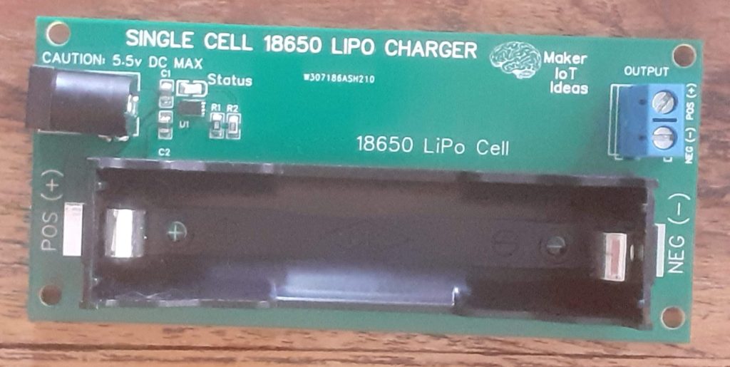
This presented me with my first problem, as absent-minded me accidently fried quite a few of them when accidentally connecting 12v to a PCB…
My solution to this was to add a Buck converter, based on my previous 3A Buck converter circuit(s) using the MP9943GQ from MPS. The buck converter can accept between 7v to 12v DC and output a stable 5.3v DC, saving me from frying chips, and also making it useable with most of the power supplies lying around in my lab – and it can also be used in the car at a later stage — Future project —
While that keeps the MCP73832T happy, and the 18650 cell charged, the next problem that presented itself was the nominal voltage of the 18650 cell itself, which is usually between 3.2v and 4.2v. In order for this voltage to be universally useful to me I needed a boost converter to increase the output to 5.15v.
This boost converter was built around the MP3423GG, also from MPS. This tiny little 14 pin IC provides the 5.15v that I need with ease, at a rated current of up to 3A. Ideal for powering other peripherals, like LDO regulators to power an ESP32 etc…

Manufacturing the PCB
The PCB for this project was sponsored by PCBWay .
Disclaimer:
Clicking on the PCBWay link will take you to the PCBWay website. It will enable you to get a $5.00 USD voucher towards your first PCB order. (Only if you sign up for a free account).
Assembly
The assembly of this PCB was quite challenging, to put it lightly. 3 QFN chips, with different pad spacing, and small sizes really tested my limits. Needless to say, proper equipment is a must, and even then, a very steady hand and good magnification will go a very long way towards ensuring success… Another option would definitely be to have the PCB professionally assembled…

A stencil is definitely required for this one, is only for that 14-pin boost converter IC, to make sure that the amount of solder paste is just right – and even then, it is still a challenge!


Summary
This was a challenging build that tested my assembly skills quite a bit. The circuit functions like intended. Now it is time to add some more features, like an ideal diode chip at the output, to allow for daisy chaining the lipo cells if required, as well as maybe a microcontroller to control power to the buck converter when the battery is not being charged.