Hi all, finally I feel like I’m making some progress with my PWM plight.
A little background:
I have the G-G-G LPSU as identified by @donkjr
I have my 2.4 pin connected to the L which is the rightmost connector on the power block [ 25v, 5v, GND, L ]
I have 2.4 configured as 2.4!^
I suspect that a lot of my problems were caused by my dodgy soldering. I can now see a PWM signal coming off my 2.4 pin [ yay ]. However if I set my config to be 2.4!^ [ inverted with a pull up ] then of course it is only being pulled up to 3.3v so when this is connected the L connector my laser still fires at power on. I can dial down the power with the potentiometer and then cut a job and can see that it’s more or less working.
So I thought I’d hook up a level shifter - this didn’t really work too well and examining the output on my scope lead to me thinking I’d done something wrong. But my mind kept drifting back to Don’s diagram with a single line coming off 2.4 and a GND wire going somewhere somehow magically working.
So @donkjr before I start delving into level shifters which I’d really rather not - can you advise on G-G-G wiring and config to work with your designs? From your page I’m convinced that…
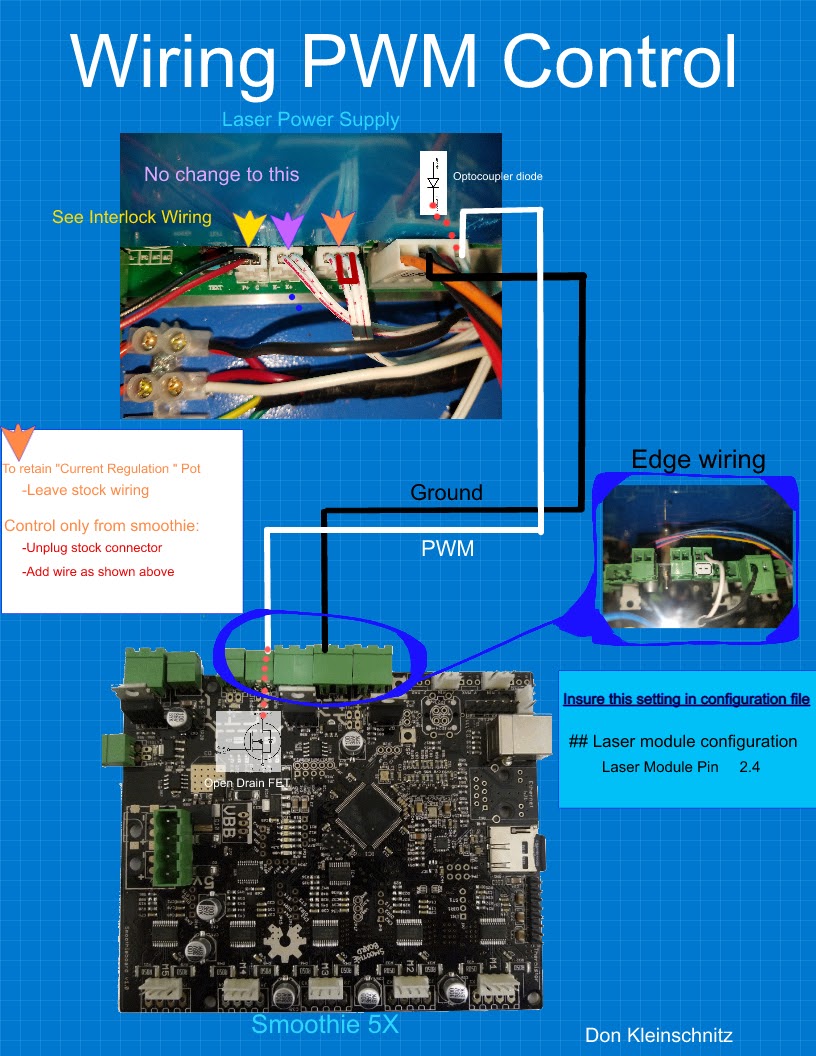
“PWM control via 'L”:
Connect the controllers PWM function through an open drain (OD) or open collector (OC) to the L pin. Choose a transistor that is connected the controllers PWM function. Insure that in your controller you configure the input to this transistor to assert in such a way that the transistor provides a ground. In other words, when PWM from the processor is TRUE the transistor should be turned on. This transistor is connected to the L pin without any form of pull-up or level shift-er. This pin from the controller will be isolated from the LPS.
In the supplies we tested this signal can be found on the rightmost pin in the LPS DC connector."
… is the stuff I’m really interested in but I’m struggling to do the final step.
You are on the right track and a level shift-er is not needed.
What board are you using?
…
The laser stays on because you have the wrong signal polarity for PWM. So whey you have the power at 90% its really 10% and when your are at 10% you are really at 90% power.
When you say you have your 2.4 pin connected do you mean from the edge connector or from an internal header?
Your K40 needs to be connected exactly like this, if you have a smoothie.
…
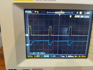
On your scope you should see a low going pulse for PWM into the “L” input on the laser power supply. Bottom trace in this picture.
…
The configuration statement in settings should be:
laser_module 2.4
Do not configure a pull-up nor invert it. -----------------------------
Some technical stuff if you want it:
When the configuration file configures a port (like 2.4) it sets up the output of the internal processor NOT the output of the driver connected to that processor port. In my setup you are employing an output MOSFET NOT the output of the processor. When the processor port goes HIGH we want the MOSFET to turn on and supply a ground, that is why it is not inverted. It does not need a pull-up as that is already included in the hardware on the board.
Ahhh, I see what you meant with your “ignore the dotted line” comment. I had the PWM coming from a pin on the board but I now see it should come off the edge of the board. It’s bedtime in the UK but I’ll give it a whirl in the morning. Thanks so much for your prompt reply.
FYI if you want an open collector/opendrain pin that is a raw pin you need to specify o (as in 2.4o) because 2.4 will actually be a pull up (no pullup or pulldown or o/c would be a - like 2.4-)
@Wolfmanjm we are using a Mosfet output as open drain to drive the PWM to the laser. So if the processors 2.4 output (which is the input to the MOSFET) is pulled up that will not impact the output of the MOSFET right?
One thing I am confused with… in this guide http://smoothieware.org/bluebox-guide#toc2
There are two L pins, one in the logic section L or TL, and one in the low power which is unconnected. Are they the same pin/function. Some people use the one in the logic section and you use the one in the low power section. Which one is best
@Wolfmanjm The “L” in the logic section and the “L” in the DC power connector internal to the supply perform the same function in the supplies that I have traced. albiet some isoltate each other using a diode
Typically the L in the logic section is used to implement the test switch.
The “L” in the DC connector is ALWAYS used for PWM as it is the signal the MOSHI boards use.
To be safe and simple I recommend that folks use the “L” in the DC because most people want a test button and some supplies don’t have a “L” on the logic section.
To reduce confusion I recommend to leave the logic section alone, use an open drain MOSFET and two wires.
I have recommended against using the raw pin because:
I wanted a MOSFET isolation from a HV ps and the processor.
Till your post I did not realize you could create an open pin on the processor port. As a result folks were using a level shift-er which creates a marginal interface to the LPS and an extra part.