Mushroom House Controller – Part 1

A Collaboration with Maesai Prasisart School, Maesai, Chiang Rai, Thailand
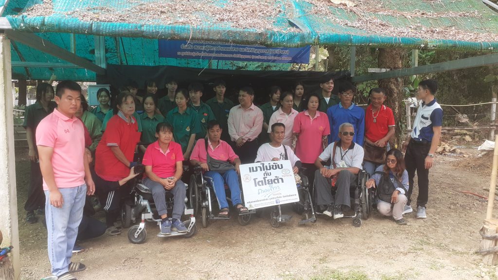
A short while ago, the local high school in my area and myself decided to collaborate on a real-world project regarding an IoT device. The device (prototype above) will be used as a controller in an Oyster Mushroom growing house, which in turn will be managed by the members of a local disabled persons association. This is very exciting for a few reasons…
I will get the opportunity to teach interested students how to solve real-world problems using electronics, as well we will do something for the community and thus contribute to making the lives of the local disabled people a bit easier.
In the long term, the data collected by the device can be used to teach other mushroom growers in the area about the optimum environment to help them ensure that they get the perfect harvest every time…
In this post, I will thus do things a little differently from my normal setup, and focus more on the collaboration, as well as teaching moments. I shall also include quite a lot of pictures. The usual schematics and PCB descriptions shall still be available, but only on the PCBWay Shared projects page ( link to be added in due course)
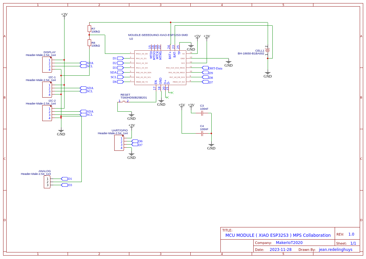
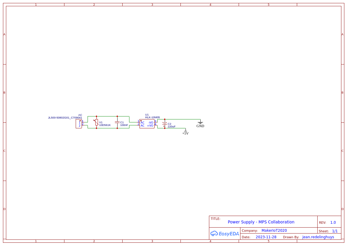
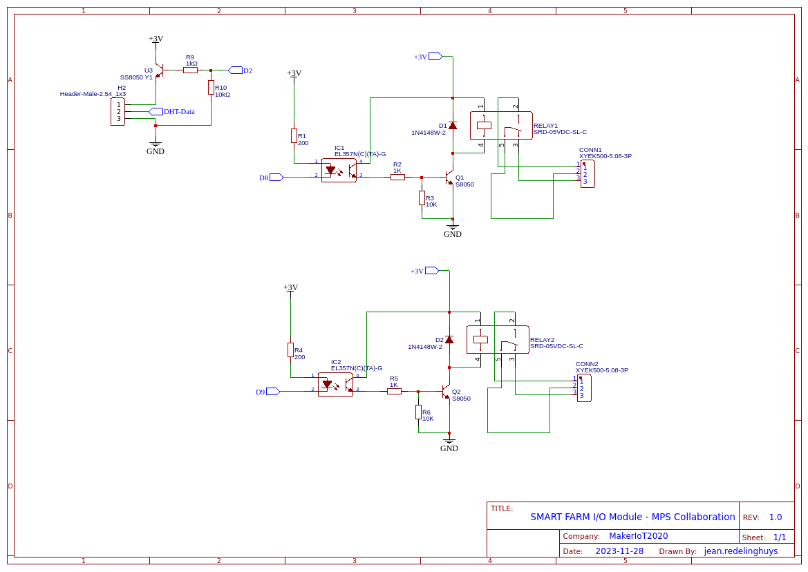
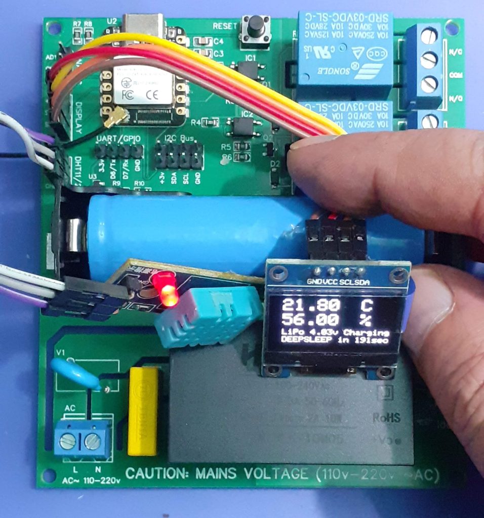
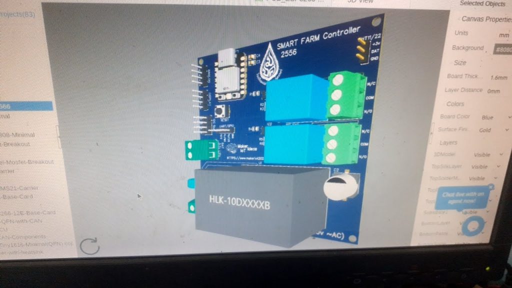
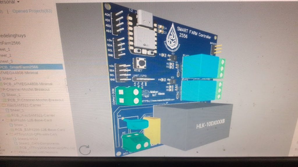
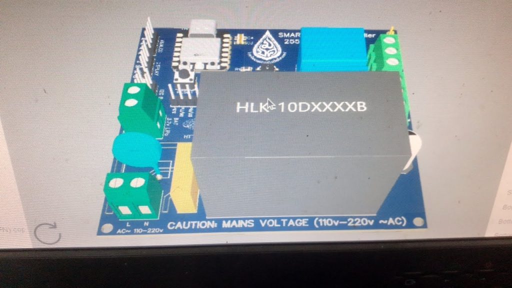
The initial idea is to produce two different PCB’s with basically the same function, for the time being designed by myself. One, used in this post, will be a 3.3v version, with battery backup, and the other will be a 5v version, with level converters ( I could not resist the potential teaching opportunity that these provided) and no battery backup. The 5v version, which I shall introduce in part 2 will be assembled by the students, while I shall assemble the 3.3v version.
Further to that, the goal is to break the PCB up into logical modules and teach the students about each module. Their task would be to then design a PCB of that module, and in the end, combine all the modules into a functional project.
As a further part to this, a special interest group shall then make use of the knowledge learnt during the development of the modules to design a third PCB including all of those modules, as well as any other that they find may be needed, assemble it and use it in the real world.
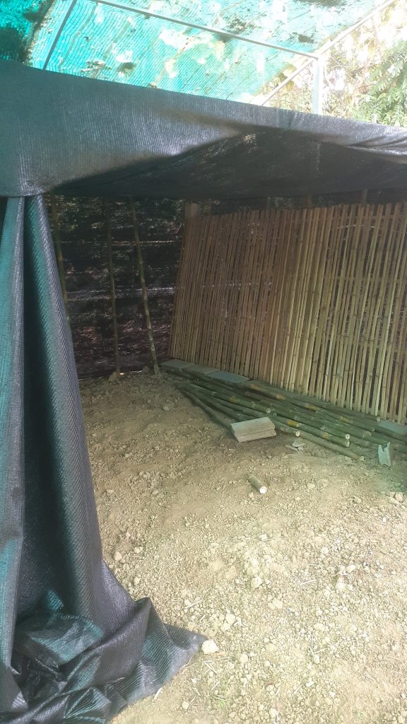
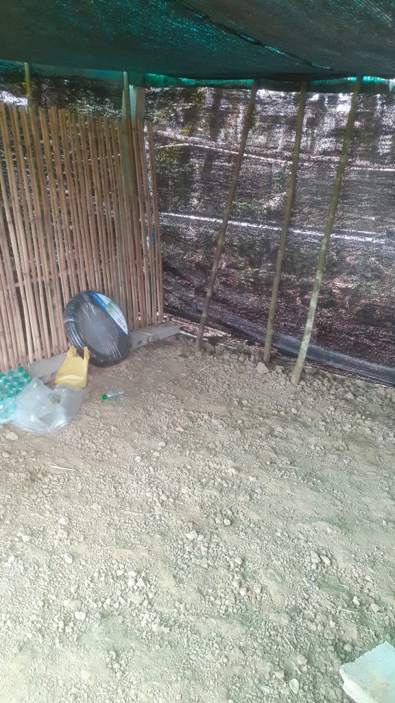
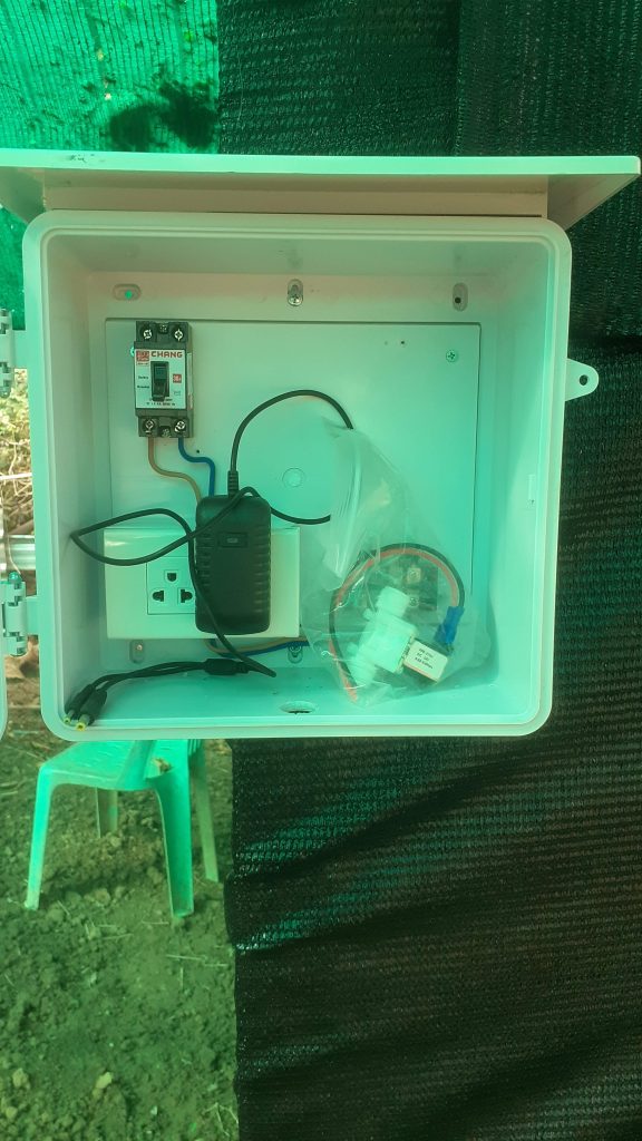
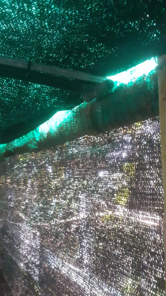
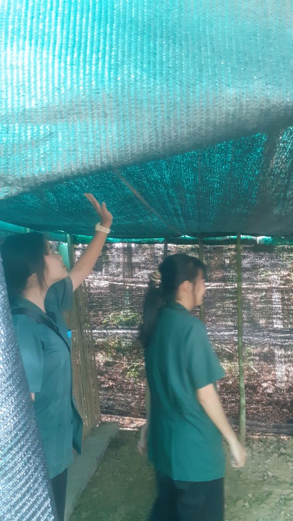
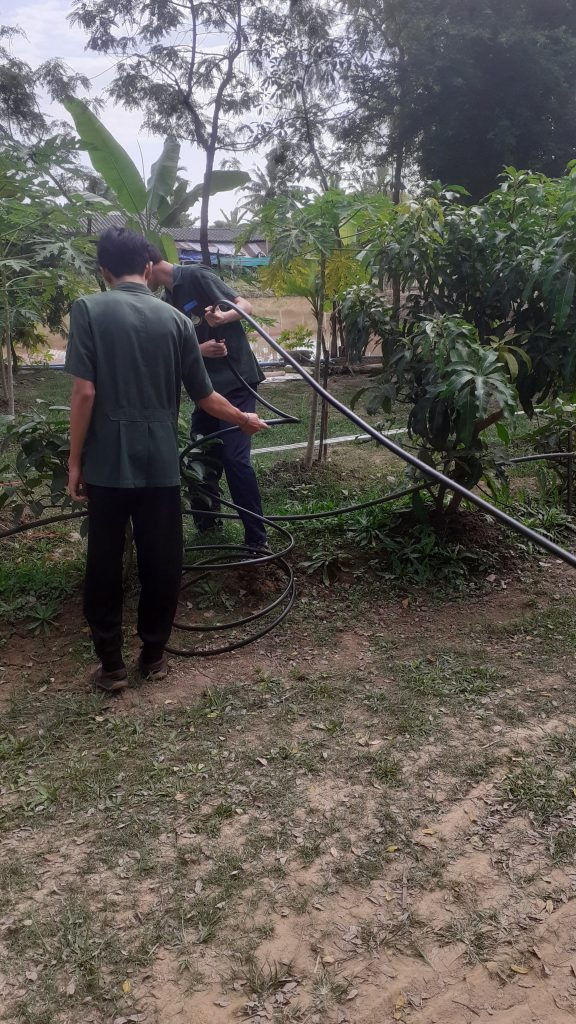
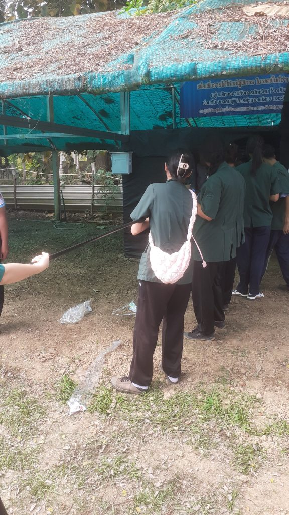
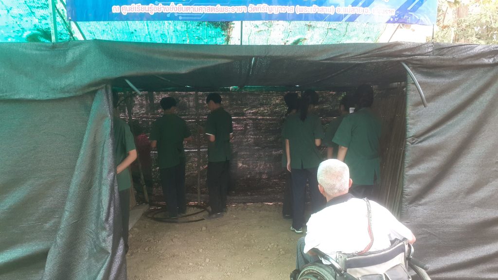
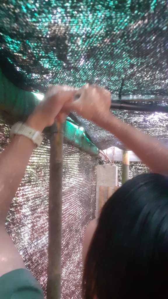
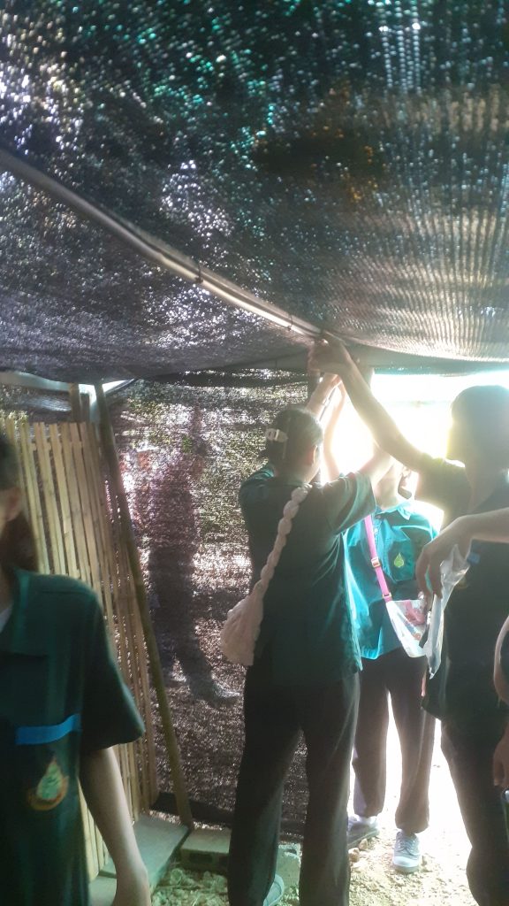
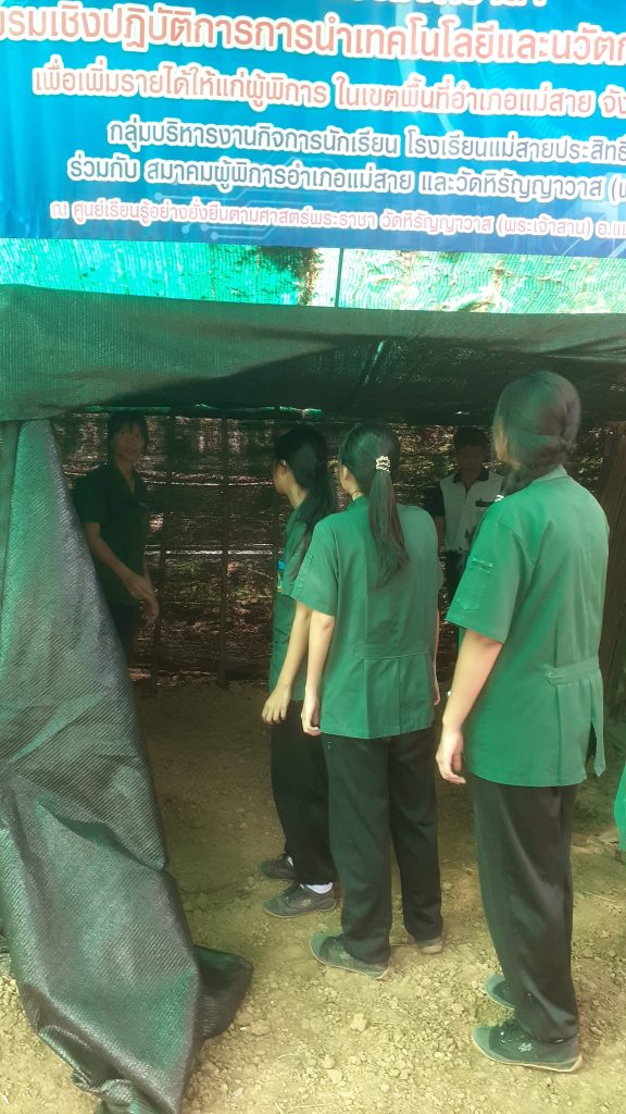
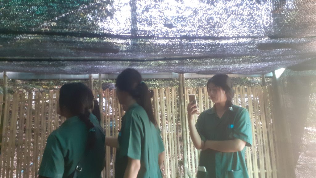
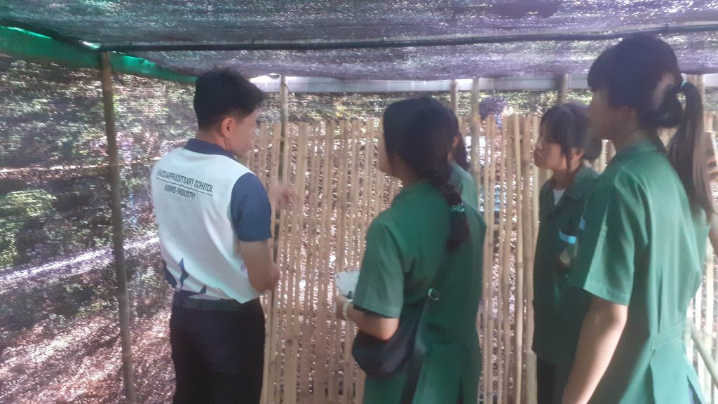
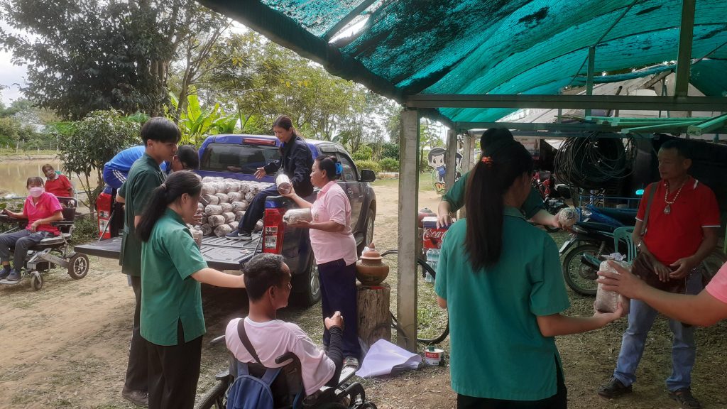
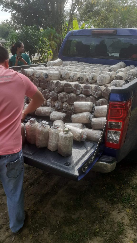
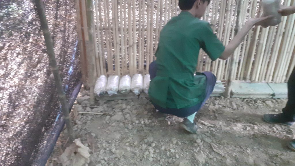
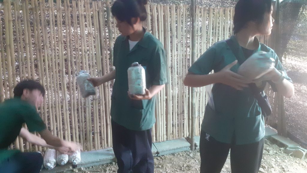
Gallery – At the remote site
Over here, Grade 12 students assist in the construction of a mushroom house.
The pictures do not need a lot of captions, as they are quite self-explanatory
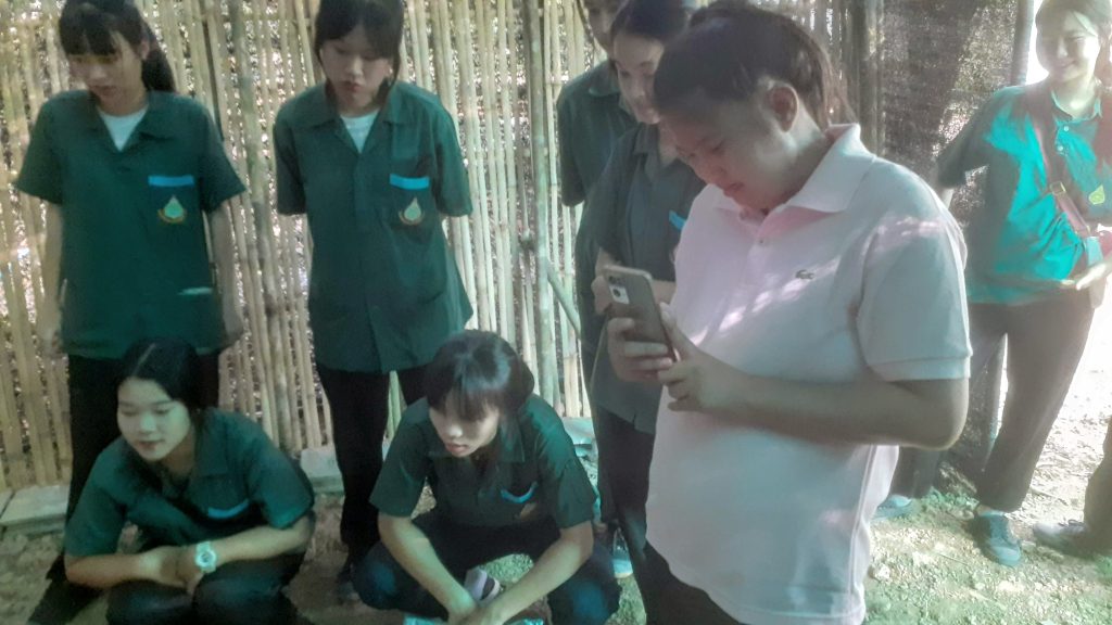
The next day, in the classroom
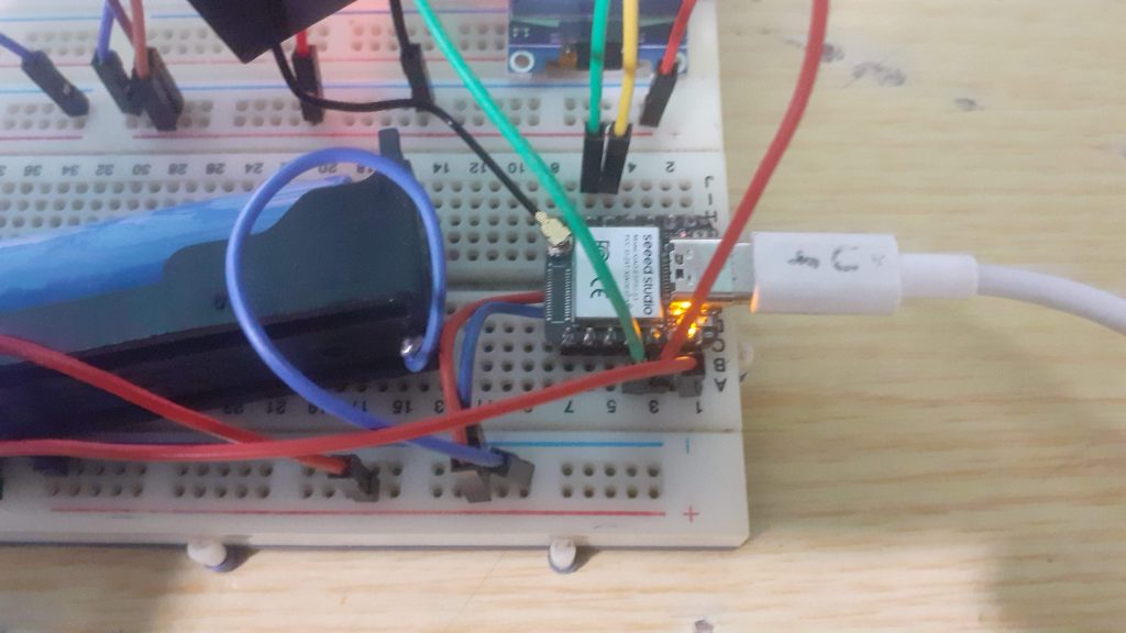
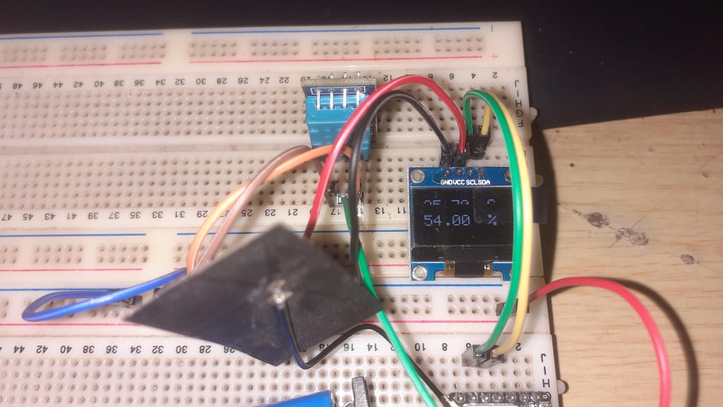
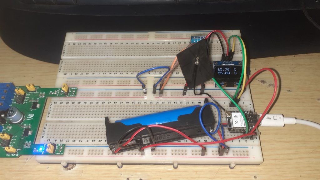
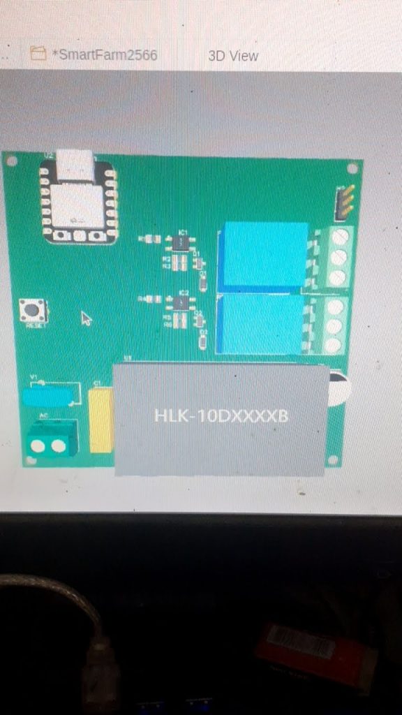
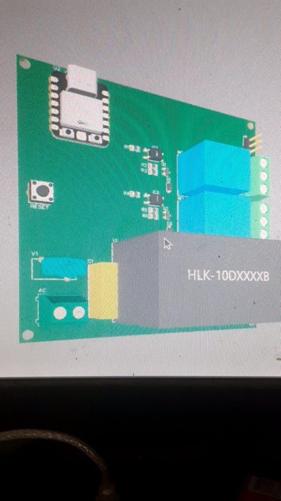
We started with a prototype on a breadboard, with some basic firmware. This was followed by a simple PCB design (with frequent 3D views so that the students could see what was happening)
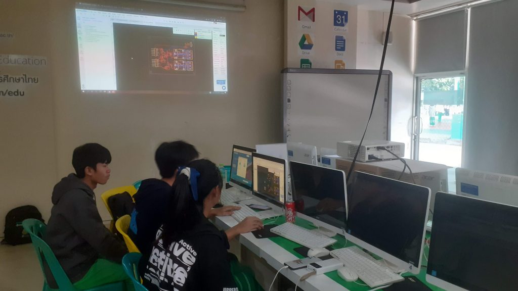
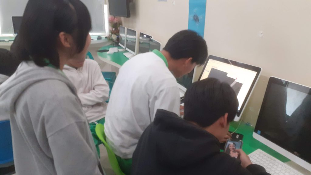
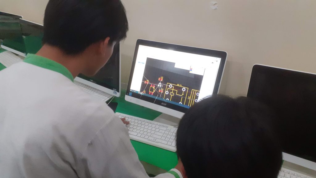
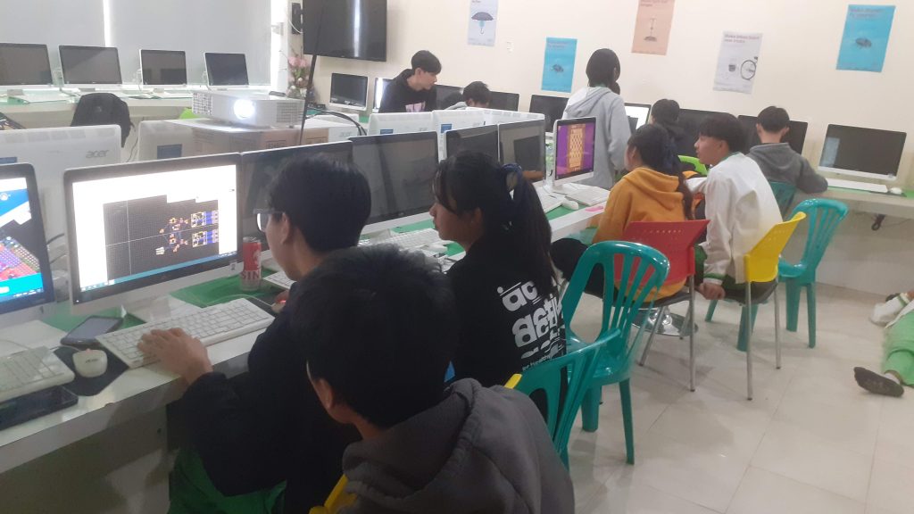
This was followed by a practical session where the students had the opportunity to try their hand at designing a part of the PCB. It is quite important that we understand that this is the very very first time in their lives that they were ever exposed to this. They were all extremely excited and some grasped the concepts quite fast, while others took a more cautious approach…
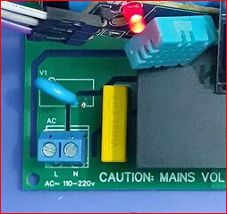
Manufacturing the PCB
Now it was up to me to finalise the initial design and get it manufactured.
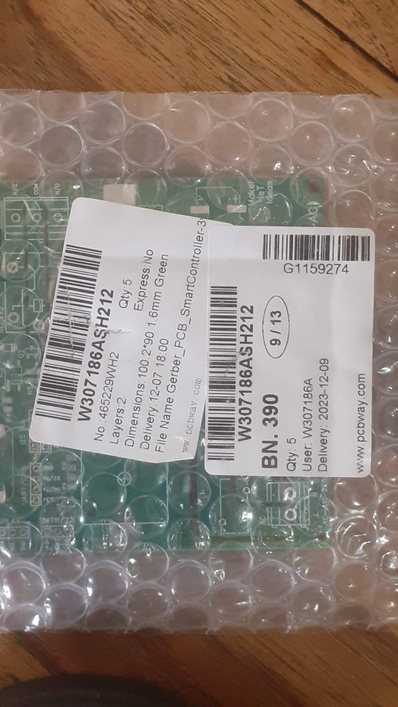
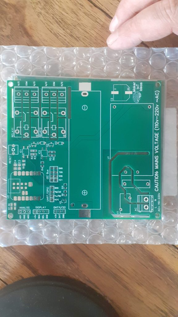
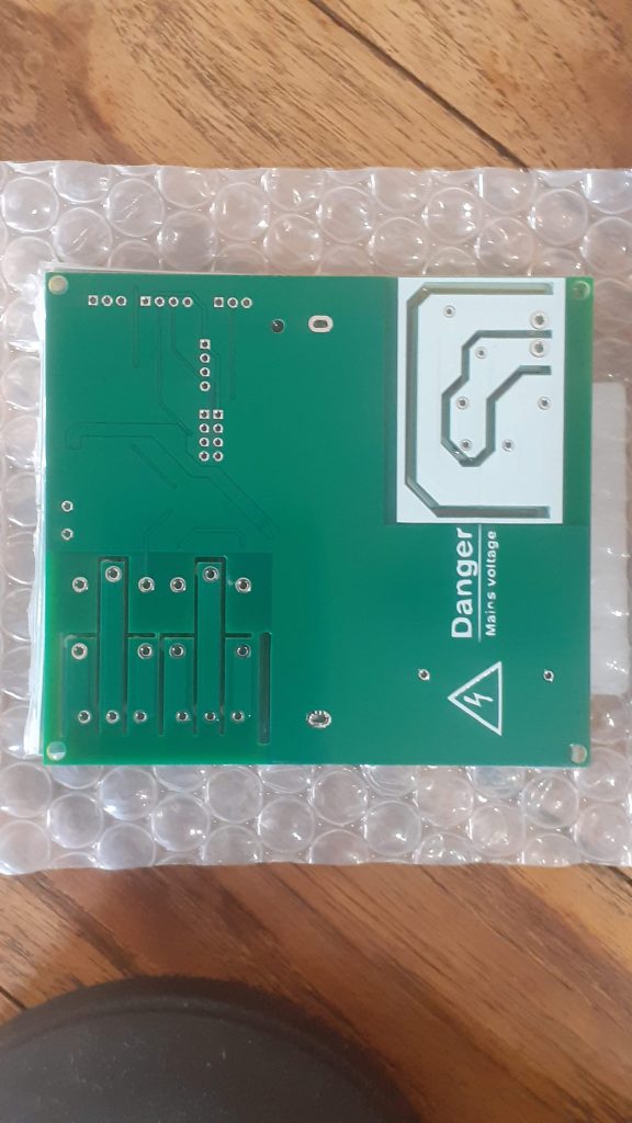
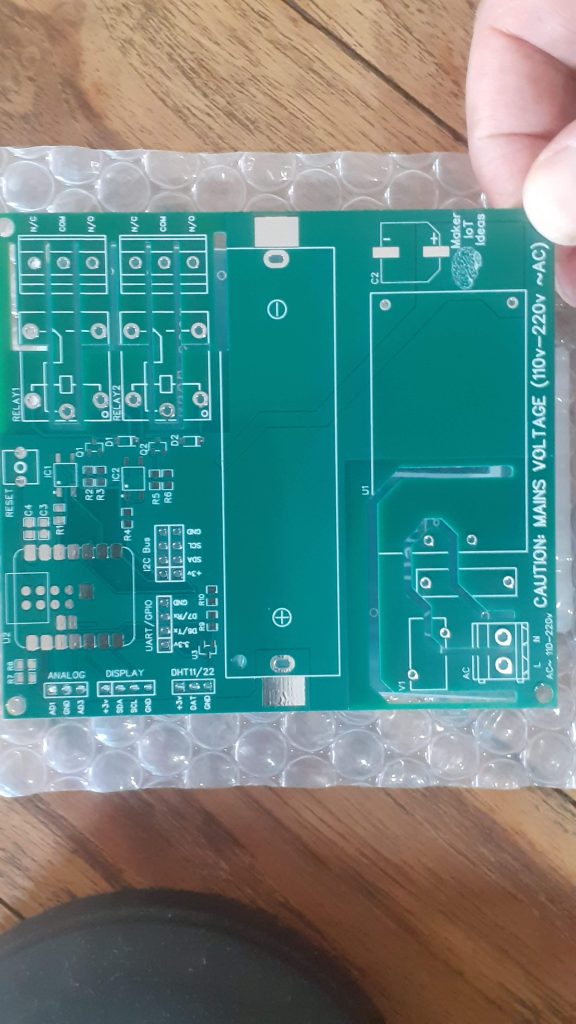
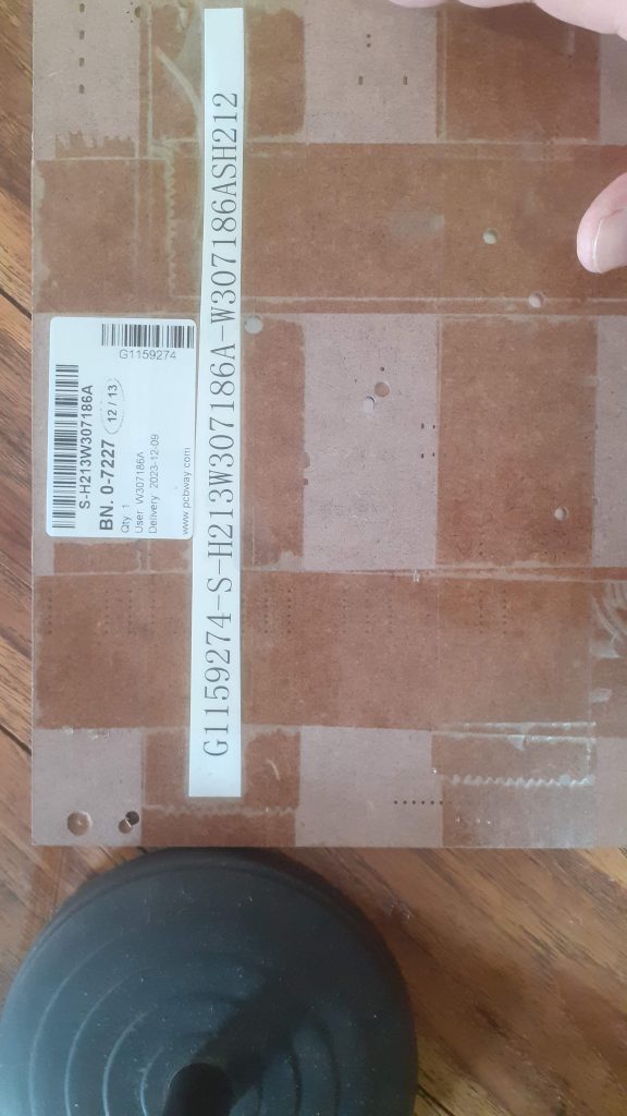
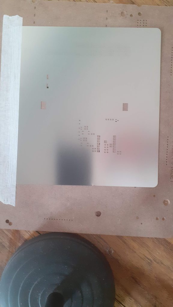
The PCB for this project was sponsored by PCBWay .
Disclaimer:
Clicking on the PCBWay link will take you to the PCBWay website. It will enable you to get a $5.00 USD voucher towards your first PCB order. (Only if you sign up for a free account).
Conclusion – Part 1
The assembly of the first board was done by myself, and firmware development was started. Stay tuned for Part 2 where the students will get the opportunity to assemble a SMD PCB for the very first time in their lives…