simple fractal algorithm would do this, maybe for heated beds also turtle grafics or some recursive function would work. The power should be calculated from the resistance (lenght, hight and thicknes of the trace). You finde some advice here https://reprap.org/wiki/PCB_Heatbed
I’d probably just do a single big double-spiral to fill the hex and then trial and error the trace widths to get the resistance. I understand it’s kind of a PITA to get the resistance bang-on though; if the manufacturer is a little over or under on the copper weight it can make a big difference.
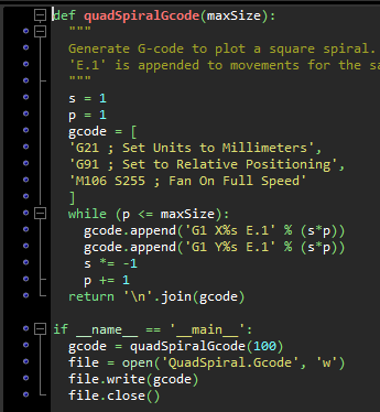
just checked, the Spirale module from my oscad library offers this - you can tweak the width and it will tell you the length (maybe the length is not right as it was intended for round spirals) - you can put two together and connect the center ends manualy - export as dxf or svg. »Spirale(grad=1200*5,radius=70,detail=100,diff=4)circle($fn=6,d=1);« missing/deleted image from Google+
I am not an electronics engineer either, but I imagine that current will be more likely to take the shortest path and as such the outer corner will get less current flow than the inner corner and that will affect where the heat is generated.
Btw, to your question of “is it a trial and error thing”, it sort of is. You can calculate what the resistance SHOULD be given the specified trace width and nominal copper thickness, but there will be some variability in these factors depending on how the board is fabricated, and if you have values that give you the right resistance from one manufacturer, even if that fab house gives you good batch-to-batch consistency (which is not a given), taking the same files to another fab house can easily give you a value that is off by 10% or more. The type of consistency that matters for making PCB heaters just isn’t what they optimize their processes for, because it doesn’t matter for more typical use cases.
@NathanielStenzel If it’s a single long trace less than a centimeter wide, it’ll probably heat evenly enough across the width of the trace without worrying too much about corners. Bigger issue will be heat loss from the edges versus center
WRT the corner cutting issue, remember that copper has high thermal conductivity, which will help keep the heat of the trace even. It also has a positive temperature coefficient, so if one part of the trace DOES start to heat more than another part, its resistance will go up, and you’ll get at least a bit more current taking the other path (though the thermal conductivity should keep this effect very small).
A bigger issue (though still smaller than the heat loss issue that Ryan brings up) is the change in effective width of the trace as it rounds a corner. For the most consistent results, the bends should be rounded, with the outer radius equal to the inner radius plus the trace width.
I guess you have to hope that the heat highs and lows get evened out well enough over the copper.
I wonder if anyone has ever taken the traces clear around the edge of the board and to the other side or along the edge for a moment and then back onto the main side or used vias to optimize heat zones.