A quick P-MOS MOSFET Driver Board
Introduction
A driver is needed to switch a P-Channel MOSFET because the gate of a P-Channel MOSFET needs to be driven to a voltage that is more negative than the source in order to turn it on. This can be difficult to do with low-voltage logic, such as 5V or 3.3V. A driver can provide the necessary voltage and current to turn on the P-Channel MOSFET, even when the logic voltage is low.
Here are some of the benefits of using a driver to switch a P-Channel MOSFET:
- Increased switching speed: A driver can provide the necessary current to charge and discharge the gate capacitance of the P-Channel MOSFET quickly, which results in faster switching speeds.
- Reduced power consumption: A driver can help to reduce power consumption by providing the necessary current in a short pulse, rather than a continuous stream of current.
- Improved noise immunity: A driver can help to improve noise immunity by providing a clean and isolated signal to the gate of the P-Channel MOSFET.
If you are using a P-Channel MOSFET in your circuit, it is a good idea to use a driver to switch it. This will help to ensure that the MOSFET is switched quickly and efficiently and that it is protected from noise.
Here are some of the different types of drivers that can be used to switch P-Channel MOSFETs:
- Logic level drivers: These drivers are designed to work with low-voltage logic, such as 5V or 3.3V. They typically have a high output voltage, which can be used to drive the gate of a P-Channel MOSFET.
- High-side drivers: These drivers are designed to provide a high voltage to the gate of a P-Channel MOSFET. They are often used in circuits where the P-Channel MOSFET is used to switch a high-voltage rail.
- Isolated drivers: These drivers provide an isolated signal to the gate of the P-Channel MOSFET. This is useful in circuits where it is important to prevent noise from entering the circuit.
Why did I decide to design this prototype?
The Story behind the prototype
This driver PCB is part of a solution for a project involving a set of 6v LED lights.
Each of the LED lights requires +/- 300mA @ 6v to operate efficiently.
I want to control these from a Microcontroller, either an ESP32 or even the XIAO RP2040 or similar. The current sink capability of an individual GPIO pin on these microcontrollers is limited, in the case of the RP2040 it is limited to 3mA per pin.
This prototype is an attempt to test out some basic driver ideas that might perform correctly for my particular needs, being
- To stay within the limitations of the particular microcontroller GPIO current specifications
- To be able to use any of the particular microcontrollers, without having to design a specific solution tailored to a specific device
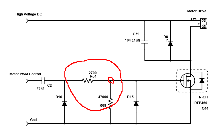
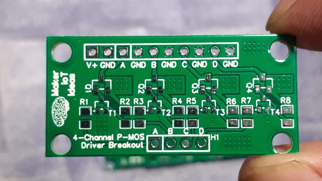
The Schematic
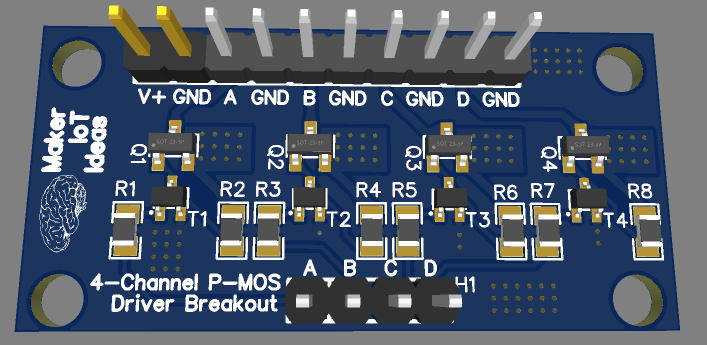
I decided to keep things extremely simple to start with, using a very simple circuit consisting of only 4 components per channel. These are :
– an S9013 NPN BJT Transistor, capable of switching up to 500mA of current
– a SI2301 P-Channel Logic Level MOSFET, capable of switching up to 2.3A
– 10k pullup-resitor
– 1k resistor on the base of the BJT
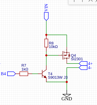
The theory of operation is as follows:
The pullup resistor, R8, keeps the gate of the MOSFET (Q4) positive, thus ensuring that Q4 stays turned off when T4 is turned off. A HIGH signal at B4 will turn on T4, which will in turn pull the gate of Q4 to ground, turning Q4 on in the process.
That will in turn turn on the load ( connected at 4+ and 4- ).
It is important to note here that the value of R8, 10K at the moment, is not finalised, and may change to increase the performance of the circuit.
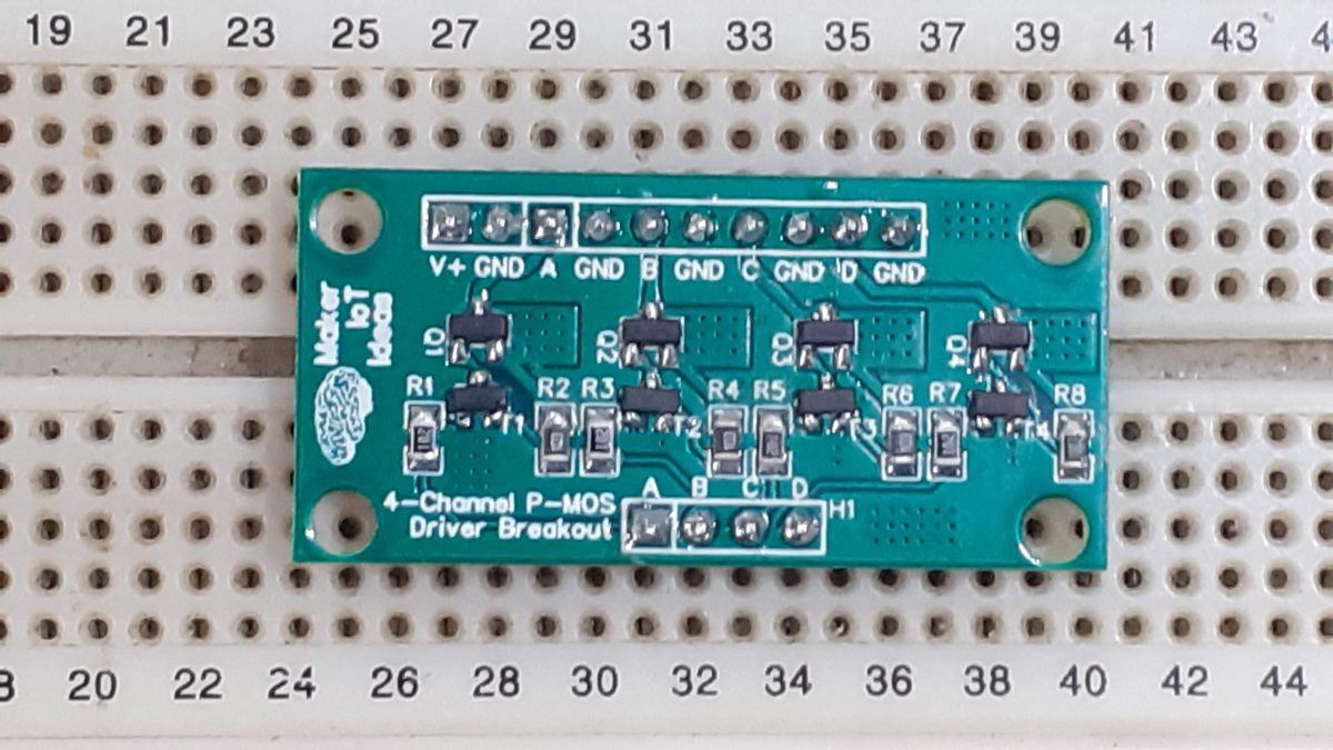
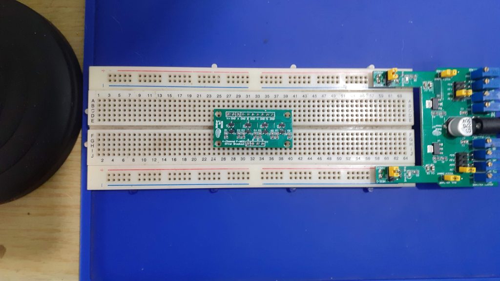
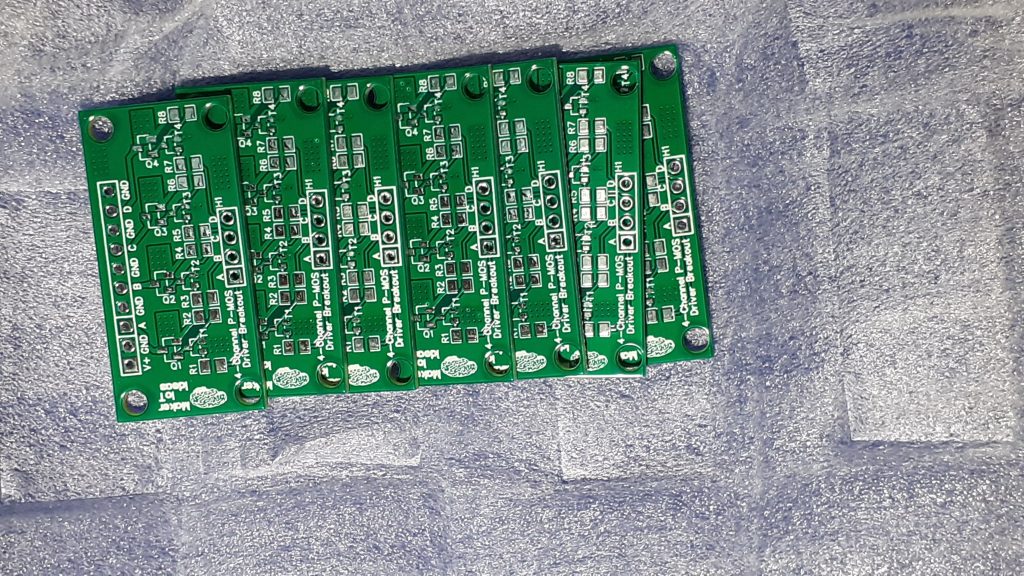
The PCB
The board was made to fit on a standard breadboard or be used as a standalone module, depending on the position of the male header pins.
Manufacturing
The PCB for this project was sponsored by PCBWay.
Disclaimer:
Clicking on the PCBWay link will take you to the PCBWay website. It will enable you to get a $5.00 USD voucher towards your first PCB order. (Only if you sign up for a free account).
I shall also receive a 10% commission AT NO COST to you if, and only if, a paid order is generated from the click on this link.
Assembly
The assembly of the PCB does not require any special tools, and can be done completely by hand if you choose. A very fine-tipped soldering iron should be perfect.
I chose to go the hot-air and solder-paste route, as it is faster, and looks neater in the end. The use of a stencil was not required.
The total assembly took about 5 minutes in total.
Testing
Testing the completed PCB module was performed with one of the LED light modules connected to each MOSFET Channel in turn, and then applying a voltage signal, or ground, to the control pin ( marked A to D on the picture above)
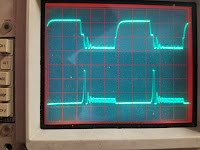
That was followed by connecting an Oscilloscope and Signal Generator to the control pins, as well as the outputs, and observing the waveforms during operation. A square wave output from the signal generator provided the switching signal.
Conclusion
The module works as expected, but the pullup resistor value needs to be fine-tuned to provide a better switching response on the MOSFET at high frequency.
I am however happy with the initial performance, and can now move on to improving the circuit to perform to my specifications.