I have a Smoothie board that shorted between traces. I suspect contamination in solder resin residue created a path for current between two terminals. I have since removed the board and cleaned the area with soap, hot water and a toothbrush. In the past, I have carefully scraped any carbonized materials out from between the traces and that’s what I did this time… very carefully.
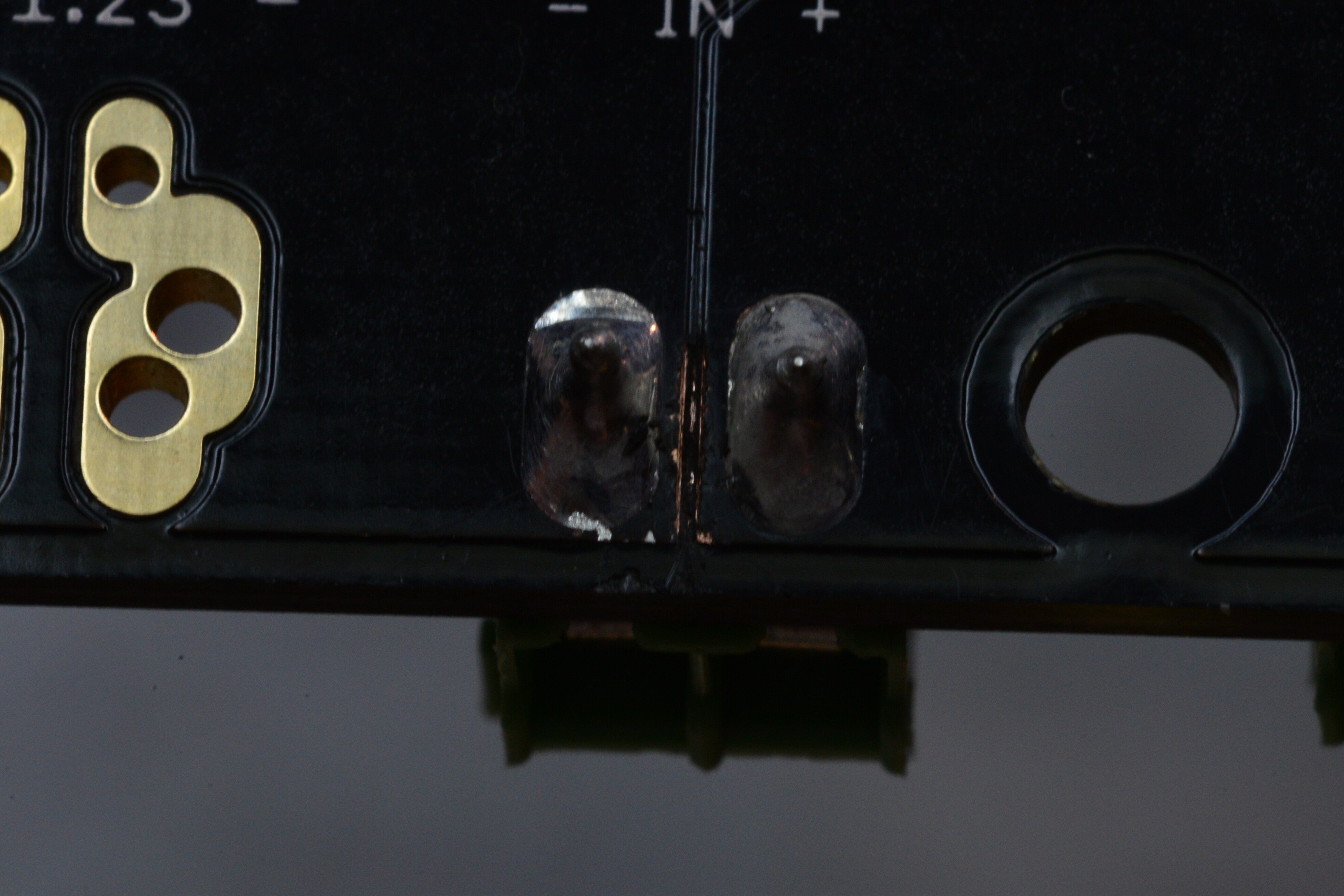
My concern is that it appears I may have exposed a copper layer below. That was a shock. I thought there would be fiberglass between layers. Am I wrong? I’ve included a picture. It shows the back side of the board below a 2 position terminal connector. You can see the exposed edges of copper from each pad… and what appears to be copper exposed between the pads where I would not expect copper!
Anyway… has anyone used something like clear nail polish or something over exposed copper like this to just give it a little bit of additional protection? I just don’t like what I see and I’m a bit nervous to leave it this way. I think the rest of the board got away unscathed.
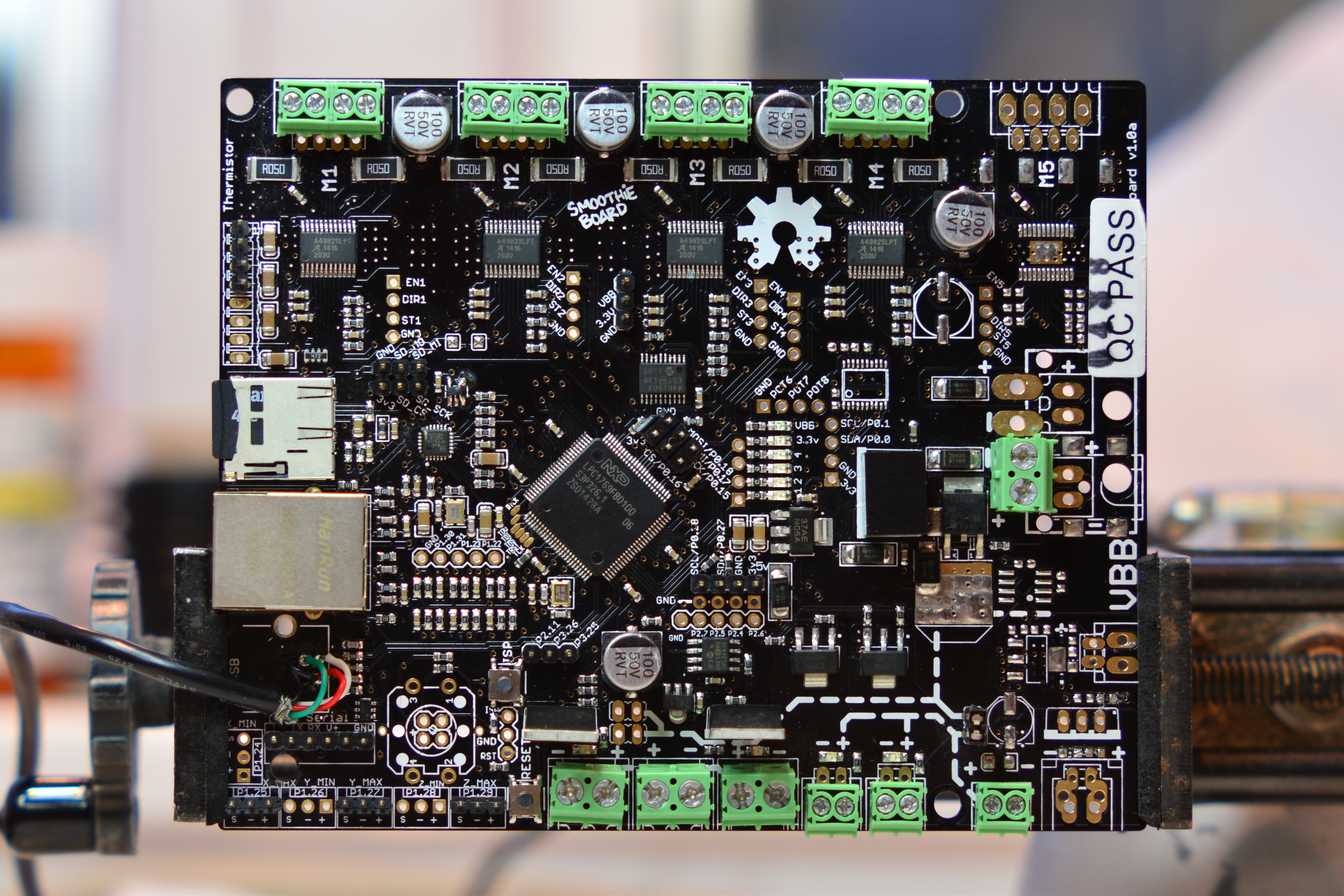
Can we get a picture of the whole board (both sides), and of any other damage you might be able to detect please?
About what’s bellow, it’s a 4 layer board, so you’ll get layers of fiber glass, and layers of copper, one on top of another.
If you mean there’s copper between the pads, that’s normal, these are entire “planes” of copper, with the pad just being a small exposed part of it. The planes are separated by empty spaces, you can pretty clearly see this in your picture if you take a step back.
If you’ve had to clean some of this up and expose copper, then clear polish or epoxy glue are definitely adequate to protect it back again.
Does the board turn on? Where is it at functionally ?
Spent some time setting up with a macro lens to get your pictures… front, back and a closer up view of the concerning area. I do notice what appears to be solder pads on top of the board that look like they overheated / vaporized (a bit). Should be somewhat visible in the closeup of the corner.
This board was on a mini delta I designed some years back. Worked great… except the “mini” magnetic end control rods would pop off if there was any bump to the head. So I pulled the board and have been installing it as an upgrade to my larger Delta from Ramps.
I’ve been in the final stages of dialing everything in using Pronterface.
I understand traces and space between. Cleaning out the carbonized crap between traces seemed to reveal copper. I stopped immediately and posted. I was expecting fiberglass board material. I’m not sure what to make of it.
I have not connected 24v to the board since this occurred. I have it connected to USB and all four green lights are on, 2 and 3 flashing. 3.3v LED is orange and on. VBB led is off.
When I connect USB to my computer it appears to work… I can see files FIRMWARE.CUR and config.txt in the printer directory and I can open config.txt.
I can not see nor smell any other suspicious areas on the board. The damage appears to be just in the corner. The arching was at the between the power input pads.
The USB cable, soldered directly to the board, was a temporary solution while I ordered the appropriate component. It has been working without problems.
I measured resistance between the two soldered pads of the terminal block (+ and -) and got 14 ohms of resistance. That doesn’t sound good.
Those are not the normal connectors, what’s going on there?
About finding copper, it’s a 4-layer board, I suspect you just got to the underlying layer. There’s really no way there’d be copper somewhere there isn’t supposed to be…
Finally, what’s up with both using the small mosfets power input and using the VBB/small mosfet jumper bridge?
Honestly, I don’t remember what I received when I first purchased this board. Did it go out with connectors? Seems like I received it bare with instructions to purchase my own. I likely used connectors I had in my own stock. They have worked fine for my purposes.
I didn’t dig into the board going through layers of fiberglass so I’m thinking the copper may be residue from the original arching. I’ll proceed on cleaning with care.
I did not use the small mosfet power input port. I installed the connector years ago but never used it. Thus the jumper.
Just trying to figure out what’s going on here… this is a 0.001%-type thing, I want to as best as possible understand what went wrong in case anything can be done to improve things moving forward (be it production or documentation ).
What kind of load did you have on each of the small mosfet output (voltage/current/hardware type) ?
I was running a 24 volt supply and the only thing I had on the small MOSFETs was a single 12v fan on the hot end. PWM control, set at 80 and controlled by the temperature switch set for 60C. I had already tested it and it was working well.