This is the preliminary layout for break out breadboards for makers to quickly expand the electronics from IC chip to solid state hardware. The plan is to produce a triangular IC chip with pin outs, with the ability to daisy chain communication, detection, and mobility shields.
Spacing between square contact pads would be the standard 2 mm o.c.
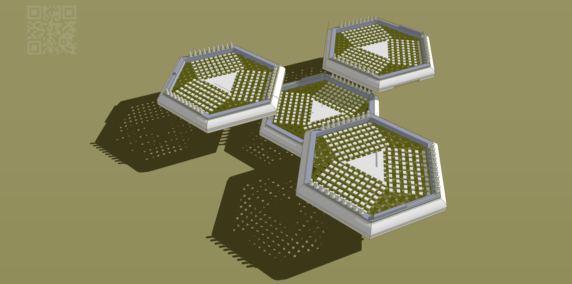
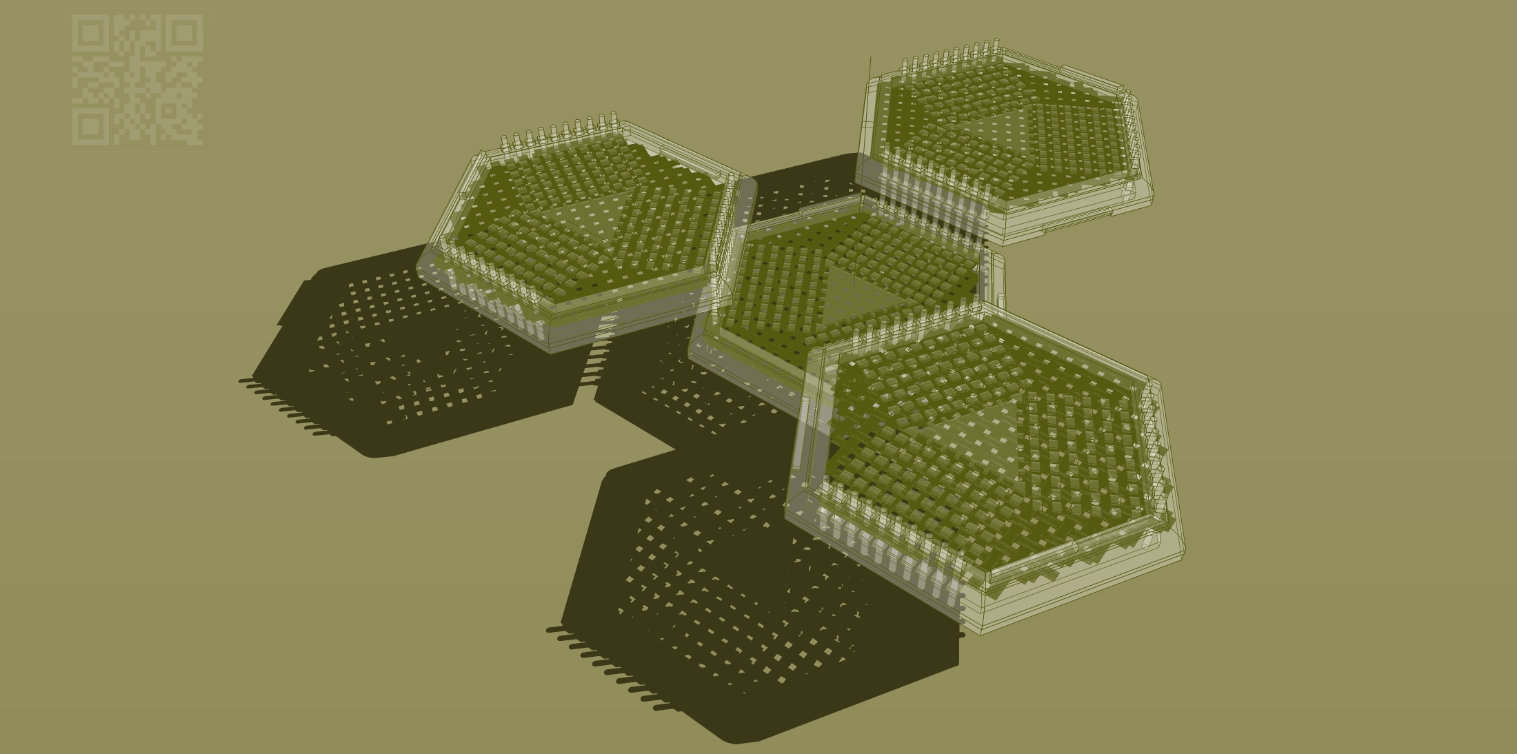
Each bagel board can be individually refined with internal layers to connect the associated contact points. The photo shows an array of 4 bagel boards, stacked like tree branches. The bagel boards can also be stacked directly on top of each other.
This would be an easy tool in teaching the youth how to breakout their electronic packages while prototyping electronic gear.
It is also an incentive to think out of the box and produce a triangular IC.
Please post your thoughts and let’s cooperate.
We are running a 3D printed prototype of this today… will post later.
“It is also an incentive to think out of the box and produce a triangular IC.” - why? Change just for the sake of change? What is the benefit of a triangular IC that is so great that it outweighs the cost of changing manufacturing methods? Why are 3 sides better than 4?
I would say the incentive would be to make it, and the manufacturing would be no more custom than the in house process developed to do it. Sometimes a maker just decides to steam punk something, with the satisfaction of making it just icing on the cake. As for a triangular com port, we could do that too… but on this one I would side with Anthony, and ask why? I would prefer standard cabling and ports on the sides of the frame.
Youth here. This looks much more confusing than your standard breadboard. Jumpers expand breadboards just fine. Jumpers also connect arduino’s to breadboards just fine.