yes, following your advises  ! will check out the SMD then, they look bigger than these small SMD resistors indeed.
oh, smaller is ok take these which fit best
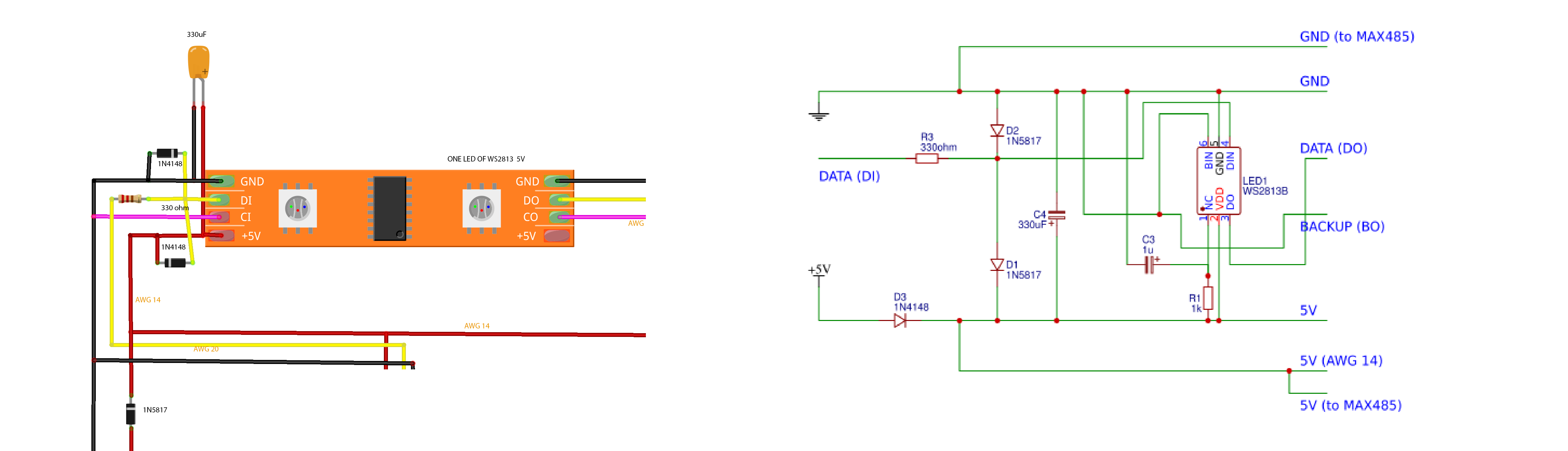
ok, so, you gave me the click to try to make a PCB out of a part of the project. in particular the part that I attached below.
Note: this is considering that everything is ok, so it is subject to changes based on your future feedback, but im trying to get my hands out of the tools 
I have no idea about the value of the capacitor C3 or the resistor R1
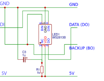
Also, I connected BI (BIN) to BO, not sure if it should be like that…
So you will see attached the part that I am trying to convert into a PCB. I think it can be interesting to learn that + it can be useful for any other project, indeed, by simply using this PCB, a LED strip will be ready to use more easily. However, I think I am facing an issue due to trace width…
With thickness of 2oz/ft², current acceptance up to 20A, it would give me trace width of approx 10mm (thats a lot haha) based on https://www.4pcb.com/trace-width-calculator.html
I used https://easyeda.com to draw the attached schematics, and now trying to do the PCB, but with 10mm width, it looks impossible…  do you think it is worth it ?
bonus question :
1-do i need a diode 1n4148 also between the max485 and esp32 ? to “hack”/fix the same 5v/3.3 similar issue?
2-will the 1n4148 be able to handle up to 18A ?!
3-having the 5 leds stripes in parallel, wont it lower the 18A to less ?
Hi @Marius_Kohsiek , I can see what you just wrote; but not the post (unless you meant this one :D)
edit : ok i see the other one now !
I just switched back to this thread
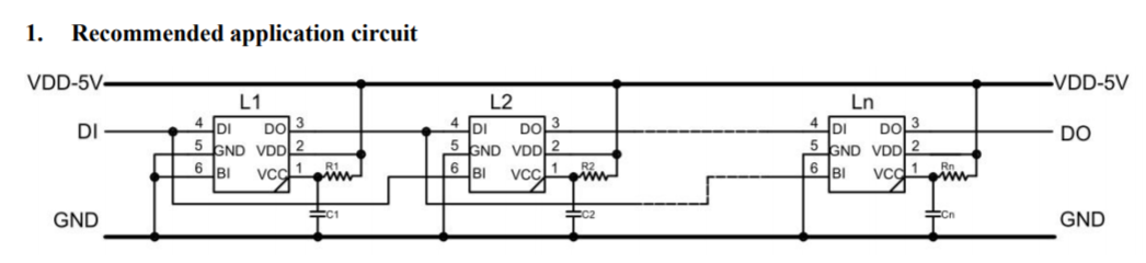
C: 6,3V is ok for the bypass capacitors since they only have to stand the 5V supply voltage. Lower rated supply voltage results in smaller packages at a given capacity. The related “best advice” often read says to put some 1000uF in parallel to a strip’s power pins. Use 330uF or 470uF at each strip I would say. It can often be read this is to compensate varying supply voltage like over shooting, but I think a good power supply serves better here. Another issue here are voltage spikes generated by the inductance over the supply lines as reaction to the pulsed current drawn by the led’s pwm circuit. To counter that problem bypass capacitors are already placed near every led on the strip usually. But adding additional capacitance near the strip is never a wrong idea though. Low impedance is adviced for bypass caps wich means tantalum or low esr electrolyte types, alternatively connect 100nf ceramic in parallel.
R: The thermal dissipation limit (the wattage) of the resistors should be irrelevant as they are placed in the data lines.
MAX485: These are differential line transceivers. One needs to be placed at each end of the line. This seems unpleasantly complicated on one hand but gives you several hundred meters of range on the other. There are cheap modules on the market at least. Google for examples and read the datasheet :).
I hope I will find time to push an updated schematic and to answer the missing questions this weekend
Greetings
@Michel_G_Khoury Hi, i have pushed a reworked schematic to the repo. I have used your sketch of the board with the strips applied to place the MAX485 modules at proper positions. Anyways, I would test if they are necessary at all, maybe transmission will work for a distance of 1m or more…
Whoa, fritzing is looking nice, but it is a buggy mess -.- If you really want to make some PCB have a look on KiCAD: http://http://kicad-pcb.org/
Answers to bonus questions:
1&2: No, the 1N4148 has the sole purpose to lower the supply voltage of the first LED by its forward voltage of 0,7V to approx. 4,3V. It therefore only needs to pass 60 mA.
3: Yes and no, on each branch there will be maximum of 18A / 5 = approx 3,6A. Supply load will nevertheless 18A max, the sum of the branches.
Missing answers from the last post:
3: DI/DO, BI/BO correct so far. The MAX485 is different, see answer for 5.
5 (and 6): MAX485, as mentioned above, are used pairwise. A’s and B’s can be connected via a twisted pair (Can be ripped of a CAT5 cable). DI is Transmitter input and RO is Receiver output, directly connected to corresponding LED pins. DE has to be high on transmitter module, RE has to be low on receiver module for setting the correct mode. Both pins have to be inverted on the opposite module.
Please let me know if you can read the reworked schematic and if you have questions about it, my friend
@Javanaut THANK YOU ! I got my mistakes, and highly appreciate your help, your answers, and your time  this is crazy !
1- max distance will be 2m, so i will stick with 1.5mm²
2- so no need for a 5v to 3.3v step down !? cool
3- for the twisted pair “data+gnd”, how to wire that ? a) i basically wire the two wires to the same pin ? or b) should i separate the wires at the end of the cables only and wire them separatly to respective pins (i.e. data to data and gnd to gnd) ? (I think its b)
4- similarly, the twisted pair for the max485 : is it : "same logic as 3 (a or b) BUT i also switch the pins for the data (i.e. pin A to pin B and B to A) ? (I think its b, and yes)
5- what do you mean by protection circuit not working well ? how do you know that it wont ? isnt that the advise from the hackaday link ? a level shifter would be for what 5v to 5v ? i dont get this one
6- regarding your notes on max485 : for the 2nd MAX485 of the 1st pair, the supply line is the same as the one of the 3rd led stripe, same for 2nd MAX485 of 2st pair and 5th led stripe, is this ok ? not sure i got it right
7- is it worth it to build the attached area as PCB ? (purpose : easier to use for future project, and cleaner + learning more) would that work out considering the 18A and 10mm trace width  ? if so, i will need to have the real ws2813 LED attached to the PCB (and not one led cut out of a stripe), and in this case, i will need to work out the wiring details of the ws2813 from the attached picture (in which case I have no idea about the value of the capacitor C3 or the resistor R1 that I mentioned earlier, we can discuss about that in details once all is done.
8- so finally, each v+ wire that will go to each led stripes will in fact only need to handle 3.6A, no 18A, correct ?
based on your answer; i think we will soon have the final version of the wiring, and i will then :
- update the github text/description/project info, add as much details as I can
- work out the PCB part and add to github
- order the stuff
- start programming and add to github to share
- create an Android app and share it as well (purpose will be to control colors/brightness/animations)
Hi +Michel G. Khoury, never mind, its just my hobby 
1: Use 1,5 mm^2 or 2 mm^2 if you are a bit worried ^^
2: The module you placed in schematic has a converter onboard… check before buy
3: b) is correct. To obtain twisted pair wire, just buy 2m of CAT5 ethernet cable in the hardware store an rip apart = 8m TP wire. See: https://4.imimg.com/data4/IY/FN/MY-10778803/1-250x250.jpg
4: Similar to 3b, but A-A and B-B, its only crossed because the modules are opposite orientated on the schematic, check their pin descriptions…
5: Well, the 1N4148 diode and the schottky diodes for protection are working against each other under circumstances, resulting in protection to minus - 0,3V/ +1,0V instead of +/ - 0,3V over/undervoltages respectively. Two 74HCT14N in series or a 74HCT245 as mentioned in https://happyinmotion.com/?p=1247 can be placed near the ESP, omitting the 1N4148 at the first LED, keeping the protection diodes and the 330 ohms in place. The ESP32 has 3,3V logic, while WS2813 and similar types run on 5V logic, a shifter needs therefore to be 3,3V->5V.
6: yes, correct.
7: Designing and making PCB is fun, just give it a try. Etching is not even necessary today (though it is fun, too) You can get 5 prototype PCB from https://www.elecrow.com/pcb-manufacturing.html for about 12$ including transport, just by sending the gerber files by email. I use KiCAD, dont mess with fritzing for pcb designing I suggest ^^ Not sure about what you mean with the attached area. However, dont route the 18A on any pcb, use the cables for that.
8: Thats true, see https://en.wikipedia.org/wiki/Kirchhoff's_circuit_laws#Kirchhoff's_current_law_(KCL)
I would buy 2 or 3 ESP32 modules (with voltage converters), the power supply, the LED strip (5m + 1m or 2m for experiments) and the passives (R,C, protection diodes) in order to build a minimum setup for testing. Depending on your current software skills programming ESP32 and even more an Android App can be demanding ventures So testing and experimenting a lot is a good idea. Eventually, when HW and SW do roughly what you want, buy the rest.
@Javanaut
im getting this passion as well now, thanks to your knowledge sharing !
1-2-3-4-8 clear !!
5- i will check out the 74HCT245 and try to find some wiring and propose something for your review ommitting the 1N4148, keeping the rest. I will still dig out a bit more to understand the - 0.3v/+1.0v explanation you mentioned, just for understanding for future reference.
6- but then why did you mention “Separate supply lines” if they are the same as the led stripes ? unless you mean separate between the two MAX485 ?
7- yep, will check out KiCAD for that. What I meant by the attached area is basically in picture attached of previous post. It is: the first led (not stripe) + capa + resistor + 2xschottky (and maybe + 74HCT245 then, instead of the 1N4148).
As the PCB will need a real LED, not a cut from a led stripe, i will need to follow some wiring as per image attached to this post, but I still dont know the C3 and R1 value.
what I mean about the 18A is because this part will be wired before the first led stripe, and will therefore have to handle high current, no ?
Hi, again Ya ya, it is a fascinating kind of technology
5: I would try the 74HCT14 first, the circuit is simpler, plus it’s a schmidt trigger, having a smaller proneness for some kind of interferences. Ok how is the 1N4148 messing with the protection circuit… I don’t know your knowledge level for electrical things, so forgive me if I tell too much basic stuff you already might know. The 1N4148s purpose is to lower the supply voltage of the first led to about 4,3V. A normal silicon diode like 1N4148 only let’s current pass in one direction. In reverse direction it will block current until a very high voltage is applied to it. Now we have 2 ways how to attach the upper protection diode: To the 5V rail or to the 4,3V generated by the 1N4148. Attaching to the 1N4148/4,3V a bad idea, as when protection diode is opening, the current will run into the 1N4148 wich will stay non conductive, leaving data in pin the only way for the current. This means there is no protection at all. Other way is to attach it to 5V, which can take up current resulting from a voltage overshooting on the data line. But problem here is, the protection diode will not get conductive before there is a potential of 5,3V on the data line (5V + 0,3V on the schottky diode). Since the supply voltage of the led is 4,3V, this is 1,0V above it, which is possibly in the harmful range. Short version: The 1N4148 is blocking the “safety path” for the current in case the upper protection diode is getting conductive (which it only does when an overvoltage condition is occuring). If this explanation is still confusing, I can draw some schematics then.
6: The other option was to use the supply lines at the end of the strips, but because there is a voltage drop along the strips, depending on the current drawn by the LEDs on this segment. This voltage would therefore not be very stable, varying probably more then +/ - 5%, as required by MAX485. An extra (separate) pair of supply wires would reduce this effect. Think of spending an extra pod to a shaky bridge making it more stable ^^
7: Hmmm, if you use a dedicated level shifter, there would not be a separate first LED? Resistor 330 ohms, the protection schottkys and the bypass cap should be placed as near as possible to the first LED of each strip. You can solder them directly to the strip or make a small PCB for that. It is still not necessary to route the 3,6A (only the main supply line before any branches is loaded with 18A) over any PCB, but nevertheless would not be harmful on such short distances. The controller and the level shifter could be placed on another PCB. R1 and C1 shown in the above schematic are not making much sense for me, as the pin they are connected to is designated “NC” which means “not connected” ^^ Each LED on a “not too cheap” strip has his own bypass cap anyways. I guess you can ignore these two components.
By the way bypass caps could be added at the additional supply lines, attached because of the MAX485s. And maybe everything is working with plain TP wires without serial drivers? On the other hand, at my last shopping tour to china (aliexpress) I replenished my stocks with 100 pieces MAX485 SOP-8 for 3€ and 50 74HCT14 for 5€ among other items =D So I personnally wouldnt think about too much before spending 4 transceivers, saving the time for a possible search for the causes of instable data transmission ^^
Greetings
@Javanaut
hi again and again
5- low level of electronics but i get your explanations ! appreciate it !
6- ok i see better now. but then, the wiring in your fritzing schematics is the other option and is correct, then no need of the extra separate supply wire you mentioned, i am right ?
7- “Resistor 330 ohms, the protection schottkys and the bypass cap should be placed as near as possible to the first LED of each strip” : each strip ??
otherwise yes, with a 74HCT14 or 74HCT245, no need of a first led, true.
ok, so my next steps :
- see the wiring changes with usage of a level shifter, and other possible points, to have a final version exactly as per reality (including the answer “each strip” in qst 7 - and maybe as well depending on answer of qst 6 !)
- try out a PCB version schematics that i will share
- go with the real wiring/soldering prior to working on the software part !
Cheers !
6: I placed the extra supply lines in the schematic, and I would use them, when possible, in your setup…
7: Bypass caps at every supply point. 330 ohms resistor at every end of a data line, that is not realized with MAX485. Protecting schottkys at the first strip and optionally at every other 330 ohms resistor.
Greetings
hi again ! quick one, coming back for some points :
1- you mentioned earlier in point 6 : “Think of spending an extra pod to a shaky bridge making it more stable” what do you mean by that ? is it an improvement to do to your schematics, or your schematics is already “up to date” for that point ?
2- we discussed earlier in point 7 that it will be 3.6A per branch, can I assume therefore that the PCB will “only” need to support up to 3.6A (so lets say 5A) ?
3- For the two 74HCT14N in series, getting there, looking for some wiring example and trying to read datasheets, patience patience
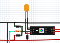
4- Regarding your answer : “R1 and C1 shown in the above schematic are not making much sense for me, as the pin they are connected to is designated “NC” which means “not connected” ^^ Each LED on a “not too cheap” strip has his own bypass cap anyways. I guess you can ignore these two components.”, please see image attached, this is where i found out about the capa and resistor
getting there with baby steps
Hiho!
1: The “extra pods” are the additional power lines for the transceivers I added to your schematic. Nothing extra to be done here.
2: With the branching of the main power line happening before any strip, max current will stay below 3,6A in any branch for sure.
3: Just connect one of its six inverters output to the input of the next building your shifter. Two general rules applying to digital circuits come into play here: Every digital/logic IC needs an 100nF bypass cap on short route parallel to supply pins. And unused inputs always need to be connected to GND (or VCC) as they could rapidly swing between states, making the whole circuit working instable then.
4: OK, R and C work as filter element here. It’s a kind of bypass capacitor with improved properties targeting the reduction of electromagnetic interference (EMI) caused by the fast switching of current by the PWM of the LEDs. In case of asking yourself how this can happen: The hard transients when switching from 0 to 60 mA in nanoseconds (switching lights on and off) is containing signal energy in the rf range. Under circumstances some meter of strip and supply lines can work as antenna for this to be radiated of But after all, these components are included in the ready bought strip, no need to worry about them.
Greetings
Hi @Michel_G_Khoury , arrived well in 2019? I am currently trying to develop a better input protection circuit for ESP8285 GPIOs Have a look here if interested. This is a source i just found, explaining some of the related issues: https://www.digikey.com/en/articles/techzone/2012/apr/protecting-inputs-in-digital-electronics
hey @Javanaut !! arrived well indeed, hope ur holidays were nice still waiting for some components to arrived before starting building some stuff ! thanks for the link and info ! would that work out for ESP32 ? how much better would that be and why ?
Hi, ya ya finally some time to relax and to be productive The shown protective measures should work for ESP32 as well for most other controllers of 5V and 3.3V types. I am using esp8285 modules currently. But the circuit shown has multiple features. For each of them it must be considered if it’s behavior is working well with your application or not. For example, the low pass filter element would probably mess up the high speed signals of a ws2812 style transmission completely. An the other hand could the features be implemented independently from each other. And it is most time advisable to do some basic calculations to adapt them a little. No need to panic, most time you come along with ohms law or something similar…
Greetings