Hey guys,
i build a laser cutter with a mks sbase and grbl as firmware. Moving works fine but now i cant get behind the secret to wire the Lase Driver with TTL correctly to the sbase. So i hope to finde the key here
I compliled grbl with the defautl ttl pin 2.5. I powered the mks with 12V, so the power on my system is fine.
With the information that I have this is where I would start.
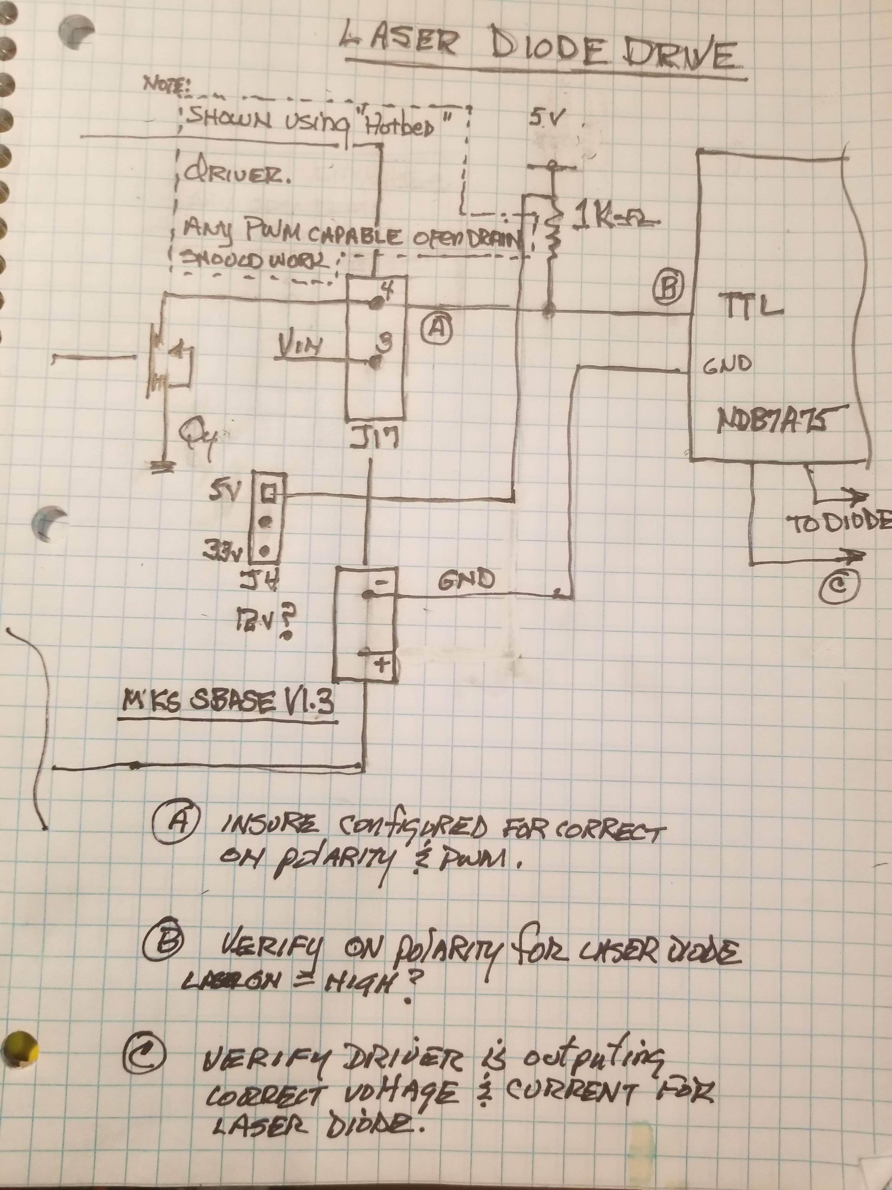
Use an open drain on the MKS board with a pull-up to drive the laser diode driver TTL input.
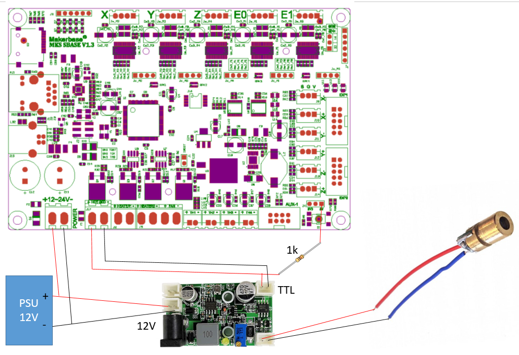
The attached hand-drawn schematic diagrams the wiring.
I do not know if the version of SYBASE that I used (see resources below) matches your board.
If not, you can modify these instructions accordingly.
Configure the SBASE board to use the Hotbed output as the lasers I/O driver.
Verify that J4-5V has 5V on it. Connect the hotbed (J17-4) to one side of a 1K resistor whose other end is connected to 5V on J4-5V.
With the machine, running verify that there is a PWM signal on J17-4.
Warning: use laser safety precautions and protect your eyes when performing this step. Verify what polarity the laser driver requires by grounding or pulling up to 5V the TTL input on the driver.
If the polarity of ON for the Laser Driver matches the SBase outputs then connect the output of the SBASE to the Laser Diode Driver and try a job! If not reconfigure the SBASE to match the Laser Diodes ON state.
Some notes on the laser diode and driver.
Ensure the driver is not set up to drive the laser diode outside its operating specification. Excessively high voltage or current will destroy the diode instantly.
I noticed that some versions of this driver have a heat sync. Ensure that you are not drawing too much current for power limits on the version without the heat sync.
The Amazon link I provided has more information on connections and user comments.
I used these resources:
*note: As an Amazon Associate I earn from qualifying purchases
Hey Don, thanks a lot for your advice.
Yes, i have the V1.3 from sbase too.
My Laser Drive have only max Output of 3mW, so i think thats the reason why there is no heatsink.
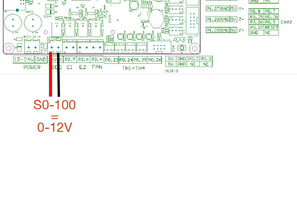
I made a quick and dirty wiring diagram. Can you have a look on it, if i understand everything right.
Ok, i did the wiring and measuring. It looks like that the TTL Output works.
I set M03 S0, the Voltage of the TTL is round about zero (but not stable?).
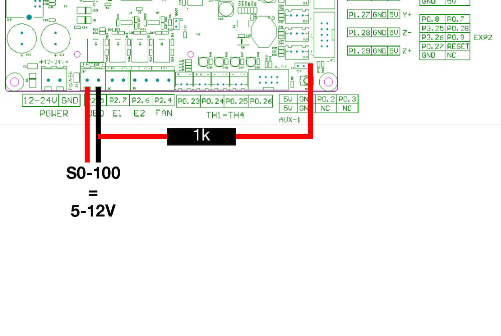
Set M03 S300 i get 5V stable. So i set S300 as my max with that i get 5V.
But, if i measure on the Laser Output of the Driver, there is no change. I always get 5V with different S Values.
Also with the Laser connected, he is fireing always with the same power.
Wait… I have had a look to your wiring diagram again.
So, did you wire the 5V J4 with the resistor to -J17 as a voltage divider?
On my diagram the 5V J4 is wired to the +J17.
So i changed it and now i can control the laser power, but in wrong direction. S0 = Full and S300=off
Does that mean i have to use P1.23 instead of P2.5?
So, did you wire the 5V J4 with the resistor to -J17 as a voltage divider?
On my diagram the 5V J4 is wired to the +J17.
The resistor pulls up the output of Mosfet Q4 (pin2*) to 5V, its not a voltage divider. The schematic does not show if pin 2 is the + or the - pin on the “Hotbed” mosfet. My guess is the + on J17 is connected to VBB (12V) not the mosfets output. I think your right the - pin is the output you want.
My screw up #1: in that I did not notice on your drawing that you have a black wire connected from J17 to the laser driver board, that is wrong. Only one wire will be connected from J17 to the TTL input of the driver.
You can verify if the correct pin is the - or the + of J17 by tracing and verifying if it is connected to the drain of Q4. You can also measure the voltage on the + pin with power on and nothing connected to it. If its connected to VBB it will read 12vdc and this is NOT the pin you want.
I do not know for certain but I think the + is probably connected to the boards VBB (+12V) so the - is the correct connection.
Do not connect anything to the other pin on J17. [I assume that is the + pin]
*My screw up # 2: J17 does not have 4 pins . It has two and they are labeled 1 and 2 in the schematic. I did get the mosfet # right as Q4.
When operating properly you should get an average voltage from J17 that is roughly proportional to the S value where: 5V is max (100%), 2.5V is 50% etc.
So i changed it and now i can control the laser power, but in wrong direction. S0 = Full and S300=off
Does that mean i have to use P1.23 instead of P2.5?
That is the wiring i understand from your sketch. So i get 6-0V (wrong direction)
Ground on the Driver Board are the same at the connectors, thats not extra wired by me.
@ManuelW
Diagram #1: measures between 12V and the PWM signal on the MOSFETS open drain. Not a relevant measure or approach especially if -Bed is not pulled up to 5V.
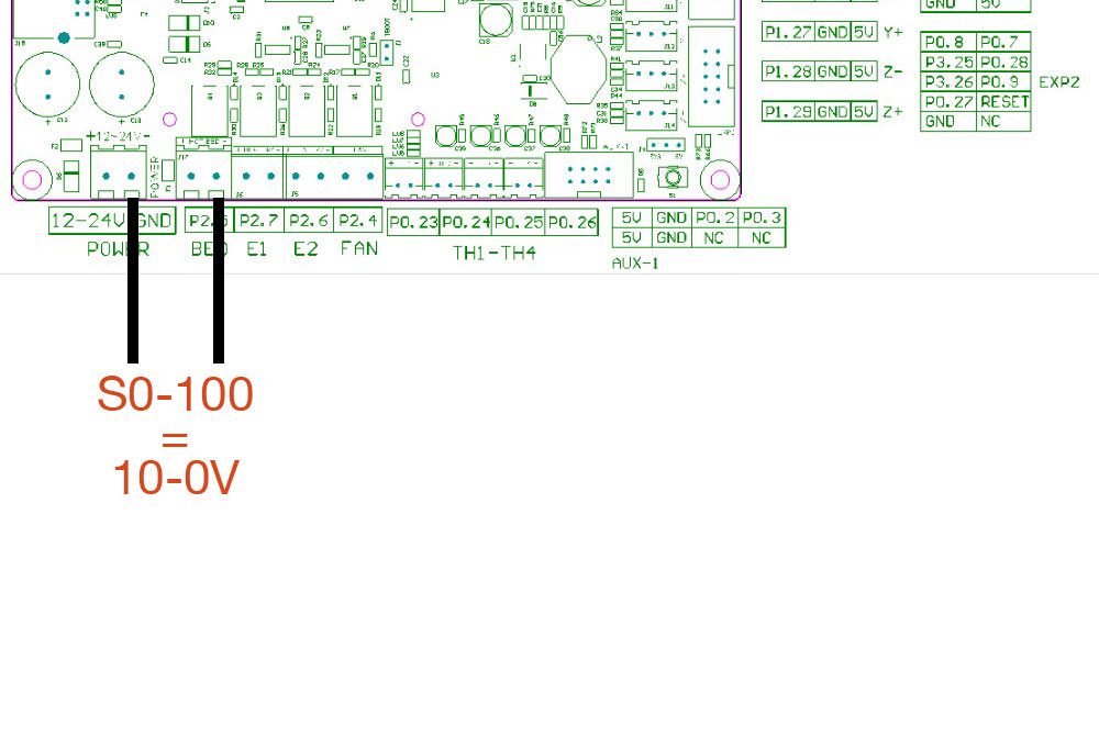
Diagram #2: measures between the ground and the open drain on the MOSFET. If the -BED was pulled up it should read 0-5 V. If not the MOSFET is floating and the reading is not relevant and undetermined.
Diagram #3:This is the correct circuit and measurement. I do not know where 6V is coming from, it should be 5V? Is the connection at J4 5V?
As I understand it, the circuit at diagram # 3 works it is just the wrong polarity for the diode driver. If you cannot invert the signal that is asserted at -Bed from the configuration file then you will have to add an inverter outside of the board. You cannot invert the signal by only changing how the diode driver is wired to the control board.
Were you not able to find a way to invert the pwm signal in the configuration file?
If not we need to think about adding an inverter to the circuit.
Hey Don, so my last Diagram with the complete wiring is correct?
I can’t find some possibility to invert the PWM Signal in the config
I found a sketch how should invert a pwm signal, but cant get it work. https://github.com/gnea/grbl/issues/22#issuecomment-341931756
OMG, i dont know what was wrong on my last try.
I did the buildup with the inverter again and oh wonder, it works
Now i get 0-4.7V in correct direction. I think the missing 0.3V does not matter?
I am the maintainer of grbl-LPC and my advise for people with TTL diode drivers would be to use a different Pin (like P1.23 on J6) and not the bed MOSFET, because the MOSFET inverts the PWM signal and grbl-LPC doesn’t have an option to invert the signal back.


